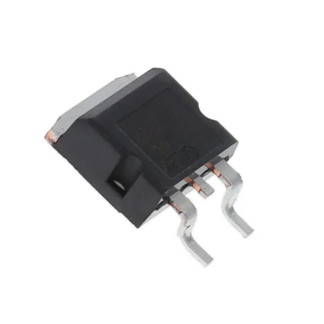
1200 V SiC Schottky — zero recovery, automotive grade
The SiC Schottky structure eliminates reverse recovery charge entirely — there is no recovery time above 500 mA forward current, which means zero switching losses in hard-switched topologies like PFC and DC-DC converters.
Forward voltage and leakage at rated current
Reverse leakage at the 1200 V blocking voltage is 120 µA, which is typical for a SiC Schottky of this die size and must be included in the thermal budget at elevated junction temperatures.
Package and mounting — D2PAK HV
The large copper tab on the bottom provides the primary thermal path to the PCB — the board copper area under the tab sets the junction-to-ambient thermal resistance. The HV variant of the D2PAK offers increased creepage distance for the 1200 V rating, which matters for high-voltage PCB layout where clearance and creepage must meet IEC/UL spacing requirements.
Junction capacitance and switching behaviour
The output capacitance measures 1650 pF at 0 V bias, 1 MHz. This capacitance charges and discharges each switching cycle, contributing to the switching loss in Coss-dominated topologies. The zero-recovery characteristic means the diode does not add a reverse-recovery charge component — the only capacitive loss is the output capacitance stored energy, which is predictable and frequency-dependent.