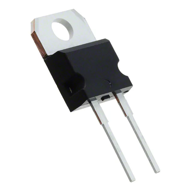
1.2 kV, 15 A SiC Schottky — the switching-loss killer
The STPSC15H12D is a 1200 V, 15 A average-rated Silicon Carbide Schottky diode in the industry-standard TO-220AC (TO-220-2) through-hole package. It uses SiC Schottky technology, which means zero reverse recovery charge — the datasheet lists a reverse recovery time of 0 ns, a direct consequence of the majority-carrier Schottky barrier. This part is built for hard-switched power stages where diode reverse recovery dominates the turn-on loss in the switch: power-factor-correction boost stages in 1 kW+ supplies, photovoltaic inverter boost sections, and high-voltage DC-DC converters. The 1200 V blocking rating gives headroom for 400 VDC bus rails with transient spikes, and the 15 A average current supports continuous-mode PFC stages well above 1.5 kW.
Zero reverse recovery — what it does for the switching loop
In a hard-switched boost converter, a silicon ultrafast diode's reverse recovery injects a current spike into the FET at turn-on that increases switching loss and generates EMI. The STPSC15H12D eliminates that spike entirely — the datasheet lists a 0 ns reverse recovery time. The practical effect is that the FET turn-on loss drops to essentially the COSS-related component, and the high-frequency ringing across the diode that forces RC snubbers is absent. For a 100 kHz PFC stage, the efficiency gain over a comparable 600 V or 1200 V Si diode is typically 0.5–1.0 % at full load, concentrated in the FET. The zero-recovery behaviour also simplifies the layout: the switching node no longer has a di/dt spike from reverse recovery that couples into the gate drive or the sense resistor. The designer still needs to manage the diode's junction capacitance (1200 pF at 0 V, 1 MHz) for the resonant tank in LLC converters, but for hard-switched topologies the capacitance is low enough that it does not dominate the turn-on loss.
Forward drop and leakage — the loss budget numbers
At 25 °C junction and 15 A forward current, the maximum forward voltage is 1.5 V. That is the starting point for conduction loss in a CCM PFC boost: at 15 A average and 50 % duty, the diode conducts for half the switching period, so the conduction loss is roughly 1.5 V × 15 A × 0.5 = 11.25 W. The actual loss at operating temperature will be higher because Vf has a positive temperature coefficient — the SiC Schottky's Vf rises with temperature, which helps current sharing in paralleled devices but increases loss as the junction heats. Reverse leakage at rated voltage is 90 µA at 1200 V and 25 °C junction. This is negligible in most applications, but leakage doubles roughly every 10–15 °C above 100 °C. At 175 °C junction the leakage can reach several milliamps, which becomes the dominant off-state loss in light-load or standby conditions. For a PFC stage that spends significant time in burst mode or at low load, the leakage at high temperature should be factored into the standby power budget.
175 °C junction — the SiC temperature envelope
The 175 °C maximum is standard for SiC power devices and significantly exceeds the 150 °C typical of most silicon power diodes. This allows the diode to survive overload conditions and high ambient temperatures inside sealed power supplies without derating the output current.
For volume pricing and lead time, submit an RFQ with your target quantity and delivery window.