Its 30 ns reverse recovery time places it in the fast-recovery class (≤500 ns, >200 mA), making it suitable for continuous-conduction-mode PFC boost stages, output rectification in flyback converters, and snubber clamping where switching losses matter.
Conduction loss and thermal budget
Forward voltage is 990 mV maximum at 8 A, which sets the per-diode conduction loss at roughly 7.9 W at full rated current.
Package and mounting — D2PAK field reality
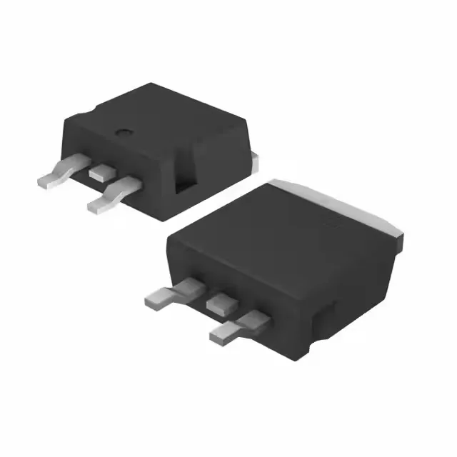
The TO-263-3 (D2PAK) surface-mount package has two leads plus the tab. The tab is the cathode connection for both diodes in the common-cathode pair, so the PCB pad must handle both the thermal and electrical connection. No lab bench needed for the swap — a hot-air station with a D2PAK nozzle and a preheat plate gets it done on site, but the tab solder joint needs a good thermal soak to avoid a cold joint.
Obsolete — sourcing reality and the replacement question
This part is listed as obsolete. No stock-holding claim; every lot is sourced per request.