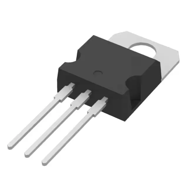
650 V N-channel in a TO-220 — what the bench sees
Gate charge is 10 nC typical at 10 V — low enough that a standard gate-drive transformer or a simple driver IC handles the switching without excessive cross-conduction loss.
On-resistance and gate charge — the switching loss trade-off
Rds(on) at 900 mOhm is specified at 2.5 A and 10 V gate voltage — the 10 V drive level is the standard for logic-level gate drivers. The 10 nC total gate charge at 10 V means the driver needs to source only about 10 nC per switching cycle — at 100 kHz switching frequency that is 1 mA average drive current, well within the capability of a TO-220 package's thermal budget.
ROHS3 compliant per. The base product number STP9N65 covers a family of voltage and current variants; the M2 suffix identifies the MDmesh™ generation.
Through-hole TO-220 — thermal and mechanical fit
The TO-220-3 through-hole package (mounting hole pattern standard to the JEDEC outline) allows a heatsink to be bolted directly to the tab. Maximum power dissipation is 60 W at case temperature — the actual dissipation in a 650 V, 5 A application is limited by the Rds(on) and switching losses, not the package ceiling.