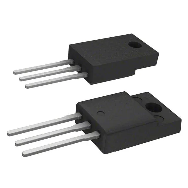
800V N-channel in a through-hole TO-220
The STP80N240K6 is an N-channel power MOSFET from STMicroelectronics' MDmesh™ K6 series, rated for 800V drain-to-source voltage (Vdss) and 16A continuous drain current at 25°C case temperature. The 220mOhm maximum on-resistance at 7A and 10V gate drive sets the conduction loss floor for a given load current — at 7A the dissipation is roughly 11W, which the 140W power-dissipation rating can handle with adequate heatsinking. The TO-220-3 through-hole package (supplier device package TO-220) is breadboard and perfboard friendly — you can solder it into a prototype board or a production PCB without reflow equipment. The three-lead layout is standard for this class of high-voltage MOSFET, so existing footprints and heatsink clips transfer directly.
Gate charge and switching drive
Gate charge (Qg) is 25.9 nC at 10V gate drive — a modest figure for an 800V device. A typical gate-driver IC sourcing 1A can switch this MOSFET in about 26 ns, though the actual rise time depends on the driver's output resistance and the gate-loop inductance. The 1350 pF input capacitance at 100V drain bias confirms the gate is not excessively large, so the drive current stays manageable even at moderate switching frequencies. The ±30V maximum gate-to-source rating gives margin above the 10V recommended drive voltage — you can use a standard 12V or 15V gate-drive rail without risk of oxide breakdown. The 4V typical gate threshold at 100µA drain current means the device is fully enhanced at 10V, but a 5V logic-level gate drive will not turn it on hard enough to reach the rated Rds(on).
Temperature range and thermal budget
The junction temperature range spans -55°C to 150°C, covering industrial and automotive ambient conditions. The 140W maximum power dissipation at case temperature 25°C assumes an infinite heatsink — in practice, the junction-to-case thermal resistance (not listed here) and the available heatsink area set the real power limit. For a 16A load at 220mOhm, the conduction loss alone is about 56W, which requires a substantial heatsink or forced airflow to keep the junction below 150°C.