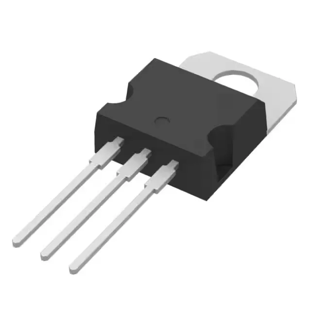
1050 V N-channel MOSFET for harsh-environment power conversion
Its junction temperature range of -55 to 150 °C qualifies it for military, avionics, downhole drilling, and other extended-temperature environments where commercial-grade parts would derate or fail.
The 10 V gate-drive voltage is required to achieve the specified maximum on-resistance; driving at lower voltages, such as 5 V, will roughly double the Rds(on), so the gate supply rail must be designed for at least 10 V. Total gate charge is 12.5 nC at 10 V, and input capacitance is 210 pF at 100 V drain bias — both figures are modest, meaning the gate driver does not need high peak current, and switching losses at moderate frequencies (tens of kHz) will be manageable. The maximum gate-to-source voltage rating of ±30 V provides margin against ringing on long gate traces.
Thermal design and mounting
The junction-to-case thermal path is the primary design constraint; the datasheet's thermal resistance figures (not repeated here) should be used to size the heatsink. The through-hole mount is straightforward for manual assembly or wave-solder lines, and the package is compatible with standard TO-220 clips or screw-mount hardware.
For BOM resilience, the MDmesh K5 family includes other voltage and current variants that share the same TO-220 footprint, but no pin-compatible second source from another manufacturer is listed in the official cross-reference data.