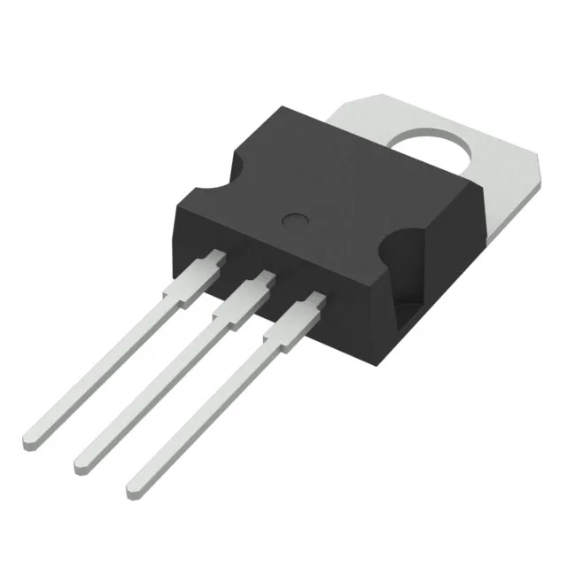
It delivers a maximum on-resistance of 24 mΩ when driven with a 10 V gate signal at 25 A load, keeping conduction losses low in high-current switching applications. With a maximum junction temperature of 175°C, it is suited for environments where ambient heat and self-heating push die temperatures high — motor drives, DC-DC converters, battery management, and industrial power supplies are typical deployment contexts.
The STP50NE08 is marked obsolete by the manufacturer. New designs should not target this MOSFET; existing BOM lines that depend on it will need to source from surplus or broker inventory or qualify a replacement. The base product number STP50N covers a family of 80 V N-Channel devices; a pin-compatible alternative within that family — or a functionally equivalent MOSFET from another vendor — should be evaluated for ongoing production. The TO-220-3 footprint is common, so a drop-in candidate with similar Rds(on) and gate charge is feasible.
The STP50NE08 requires a 10 V gate drive to achieve the rated 24 mΩ Rds(on). Maximum gate-source voltage is ±20 V, so the driver rail must stay within that window. Gate charge is specified at 110 nC at 10 V, which gives a reasonable switching speed for hard-switched topologies at moderate frequencies — a gate driver capable of sourcing and sinking a few amperes peak will keep transition times short. Input capacitance is 5100 pF at 25 V drain-source, a figure to budget for in the gate-drive power calculation and switching loss estimate.