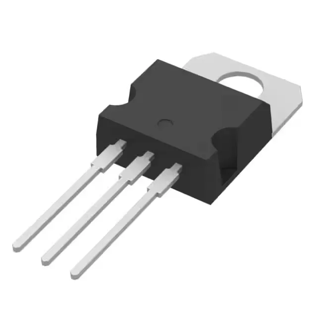
650 V N-channel MOSFET in TO-220 — MDmesh V platform
139 mOhm on-resistance — conduction loss budget
This is the figure to use for worst-case conduction loss calculations at full load and high junction temperature — the datasheet's typical curve will show a lower value at 25°C, but the 139 mOhm max at 11 A is the number for thermal design margin. Gate charge totals 64 nC at 10 V, which sets the drive current needed at the target switching frequency. A 64 nC gate switched at 100 kHz draws 6.4 mA average from the gate driver — well within the capability of most half-bridge driver ICs, but the peak current capability of the driver must still source the Miller plateau charge in the switching interval.
Input capacitance and switching edge rates
Input capacitance Ciss is 2880 pF typical at 100 V drain-source bias. This capacitance, together with the gate resistance and driver impedance, sets the turn-on and turn-off delay times. For hard-switched topologies like PFC or LLC half-bridge, the 2880 pF Ciss is moderate — it does not require a heroic gate driver but does call for a gate loop layout that minimises parasitic inductance between the driver output and the TO-220 gate pin.
Thermal and mounting — TO-220 tab considerations
Maximum power dissipation is 140 W at case temperature Tc=25°C, derated to zero at 150°C junction.