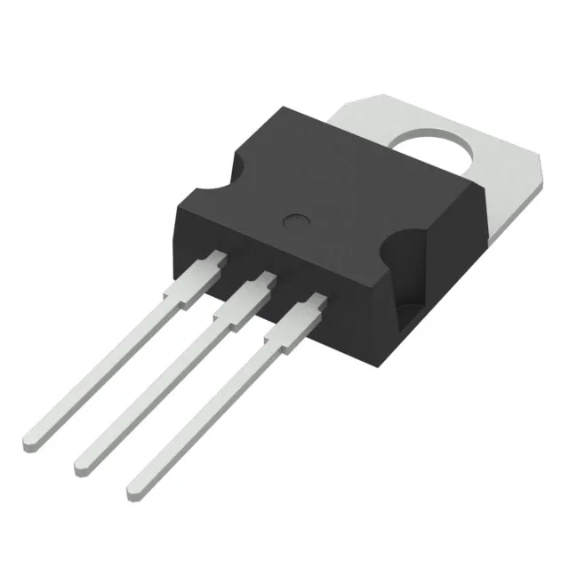
The 4.6 nC typical gate charge at 5 V and 475 pF input capacitance at 25 V drain bias mean the gate driver sees a light capacitive load, keeping switching losses low in hard-switched topologies.
Obsolete — plan the last-time-buy or cross now
No successor order code is listed on the official record. For a production BOM that still calls out this exact MPN, the practical path is a last-time-buy through the remaining independent-distribution channel, or a qualification exercise to a pin-compatible 30 V N-channel TO-220 MOSFET from the same STripFET family or an alternate vendor. The TO-220 footprint is a common baseline, so a parametric cross should be straightforward, but the gate charge and Rds(on) numbers need matching to preserve the switching performance in the existing design.
Gate charge and input capacitance — why they matter for the switcher
The 4.6 nC gate charge at 5 V and 475 pF input capacitance at 25 V Vds are the figures a power-supply designer reads first after the on-resistance. A low gate charge means the driver can switch the FET quickly without needing a high peak current, which is valuable in high-frequency DC-DC converters where dead-time losses eat into efficiency. The 20 mOhm Rds(on) at 10 V drive is the headline number, but the drive voltage range is specified from 4.5 V to 10 V, so the part can be driven from a 5 V logic rail with some Rds(on) penalty — the 4.5 V minimum drive voltage is worth checking against the gate-drive supply in the schematic.