650 V, 18 A — the switching load line
The STP20N65M5 is an N-channel MOSFET from STMicroelectronics' MDmesh™ V series, rated for 650 V drain-to-source voltage and 18 A continuous drain current at 25°C case temperature. That 650 V ceiling puts it squarely in the 600–650 V class for offline flyback, PFC boost stages, and resonant converters where the drain sees the reflected output plus leakage spike — the 50 V margin above a 600 V rail gives some headroom for ringing.
On-resistance and gate drive — the switching loss trade
Rds(on) is 190 mOhm maximum at 9 A drain current with 10 V gate drive. That is the conduction loss figure for the BOM — at 9 A the dissipation is I²R ≈ 15.4 W, which against the 130 W package limit (Tc) leaves thermal margin for switching losses. The gate charge is 45 nC at 10 V; a typical gate driver sourcing 1 A charges the gate in about 45 ns, so the switching transition is fast enough for 100 kHz hard-switching without excessive cross-conduction. Input capacitance Ciss is 1345 pF at 100 V drain bias. That is the load the gate driver sees during the Miller plateau — a driver with 2 A peak current capability will slew the gate through the plateau in roughly 25 ns, keeping the switching edge clean. The ±25 V maximum gate rating means a standard 12 V or 15 V gate rail is safe; the 5 V threshold at 250 µA ensures the device is fully off with a 0 V gate.
Through-hole TO-220 — the repair-bench favourite
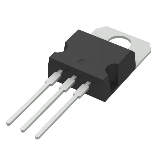
The TO-220-3 package with through-hole mounting is a repair-bench staple — the tab solders to the board or clips to a heatsink, and the three leads are easy to probe, desolder, and replace. The operating junction temperature range is -55°C to 150°C, covering industrial and automotive under-hood environments. The tube packaging means it ships in anti-static tubes, not tape-and-reel, so it is suited for hand-assembly or low-volume production runs.