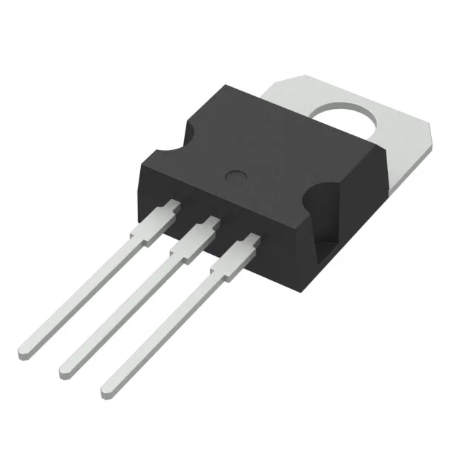
STMicroelectronics STP19NM50N — Discrete Semiconductors

STMicroelectronics STP19NM50N MOSFET

MPNSTP19NM50N
Active

STMicroelectronics STP19NM50N, MDmesh™ II series, N-channel MOSFET, 500V Vdss, 14A Id, 250mOhm Rds(on), TO-220-3, Tube.

$3.9800Ref. price · indicative, final on quote
PackagingTO-220-3
RoHSROHS3 Compliant
SeriesMDmesh™ II
Independent supplier — new & surplus stockAuthenticity-screened · ESD-safe packingListing updated Aug 2026

Specifications

STP19NM50N specifications
ParameterValue
SeriesMDmesh™ II
FET typeN-Channel
MountingThrough Hole
Drain to source voltage500 V
Drive voltage (Max rds on, min rds on)10V
Current - continuous drain (Id) @ 25°C14A (Tc)
Power dissipation110W (Tc)
Operating temperature150°C (TJ)
PackageTube
Vgs±25V
TechnologyMOSFET (Metal Oxide)
CaseTO-220-3
Vgs(th) (Max) @ id4V @ 250µA
Rds on (Max) @ id, vgs250mOhm @ 7A, 10V
Gate charge (Qg) (Max) @ vgs34 nC @ 10 V
Input capacitance (Ciss) (Max) @ vds1000 pF @ 50 V

Product details

500 V N-channel MOSFET in TO-220 — the switching load envelope

The STP19NM50N is a 500 V drain-source, 14 A continuous-drain N-channel MOSFET from ST's MDmesh™ II series, packaged in a through-hole TO-220-3. These numbers set the gate-driver current requirement: a driver sourcing 1 A can charge the gate in about 34 ns, though the practical switching speed is also limited by the gate-drive loop inductance and the external gate resistor.

Active lifecycle — still a current-production MOSFET

The part is ROHS3 compliant, meeting EU Directive 2011/65/EU and its amendments for lead-free soldering processes. The base product number is STP19, which covers the TO-220 variant in the MDmesh™ II family.

Parametric fit — what the ratings mean for the BOM line

The 500 V Vdss and 14 A continuous current cover a wide range of offline power-converter topologies — flyback, forward, half-bridge — where the MOSFET sees the rectified mains plus reflected voltage. Maximum junction temperature is 150 °C. The 110 W power dissipation at the case (Tc) assumes an infinite heatsink; in practice the TO-220 package's junction-to-case thermal resistance (not listed here) drives the derating, so the actual continuous power is limited by the heatsink's thermal impedance and the ambient temperature. Gate threshold voltage (Vgs(th)) is a maximum of 4 V at 250 µA drain current. This is the point where the device just begins to conduct — for a 10 V drive, the gate overdrive is 6 V, which keeps the Rds(on) in the specified range. The ±25 V maximum gate-source rating gives margin for ringing on the gate node in a hard-switching converter.

Frequently asked questions

What is the closest second-source for the STP19NM50N?

The closest functional peers from ST's own portfolio are the STP18N65M2 (650 V, 12 A, 330 mOhm), the STP18N60DM2 (600 V, 12 A, 295 mOhm), and the STP15N65M5 (650 V, 11 A, 340 mOhm). All are N-channel TO-220 MOSFETs with ±25 V gate drive and 150 °C junction rating. The STP18N65M2 is the nearest match in Rds(on) and gate charge (20 nC vs 34 nC), but the drain current and voltage ratings differ — verify the BOM's voltage margin before substituting.

What compliance documentation does STMicroelectronics provide for the STP19NM50N?

The STP19NM50N is ROHS3 Compliant. The manufacturer provides a datasheet with electrical characteristics, a material declaration, and a PCN notification channel for any changes to the product or process.