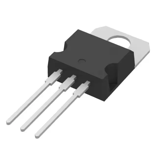
200 V, 15 A N-channel MOSFET in TO-220
The STP19NF20: The 200 V Vdss rating sets the bus voltage ceiling for the application — suitable for 48 V telecom rectifiers, 72 V battery banks, and 120 V or 170 V DC-link rails in motor drives and power supplies, with margin for transients. The 160 mOhm maximum on-resistance at 7.5 A and 10 V gate drive defines the conduction loss floor. At 15 A, the I²R loss at the rated current is about 36 W, which aligns with the 90 W power dissipation capability at the case — the part runs hot but stays inside the SOA with adequate heatsinking. The TO-220-3 through-hole package (supplier device package TO-220) mounts into a standard 0.100-inch pitch footprint on the PCB or a clip-on heatsink, common in off-line power supplies and DC-DC converters.
Gate drive and switching profile
These numbers tell the gate-drive designer what the driver must supply: a gate-drive current of 0.5 A charges the gate in about 48 ns, so a standard 1 A gate-driver IC handles this comfortably at switching frequencies up to 100 kHz. This means the MOSFET does not fully turn on with a 5 V gate drive — it requires the full 10 V to achieve the rated Rds(on). For designs using a 12 V gate-drive rail, the 4 V Vgs(th) provides good noise immunity; the device stays off until the gate voltage exceeds 4 V, which is well above typical ground-bounce levels.
The junction temperature range spans -55°C to 150°C, covering industrial and automotive ambient conditions. The 150°C maximum junction temperature is standard for power MOSFETs; the thermal design must keep the junction below this limit at the worst-case load and ambient. The 90 W power dissipation at the case assumes a case temperature of 25°C — in a 70°C ambient with a 1°C/W heatsink, the allowable dissipation drops to about 45 W, which still accommodates the 36 W conduction loss at 15 A.