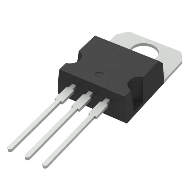
1050 V N-channel — MDmesh K5 for high-voltage switching
The 21.5 nC total gate charge at 10 V means a standard gate driver IC can switch it at 100 kHz without excessive drive current — figure about 2.15 mA per 100 kHz from the driver output. This combination of high voltage, moderate current, and low gate charge targets offline flyback and PFC stages, solar inverter boost converters, and auxiliary power supplies where the primary-side switch sees rectified 400 VDC bus plus ringing margin.
Junction temperature range and thermal budget
The 5 V gate threshold at 100 µA drain current is a maximum — the typical threshold is lower, but the design must guarantee 10 V gate drive for the rated Rds(on). Below 10 V the on-resistance rises sharply, and the part may not fully enhance at 5 V gate drive.
Input capacitance and switching speed
Input capacitance (Ciss) is 545 pF maximum at 100 V drain-source. That is low enough that the switching losses at 100 kHz are dominated by the gate charge, not the Miller plateau duration. The 30 V maximum gate-source rating gives headroom for gate-drive overshoot — but keep the ringing below that absolute maximum, not the nominal drive voltage.