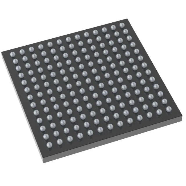
STMicroelectronics STM32L4A6AGI6 — Microcontrollers & Processors (MCU / MPU / DSP)

STM32L4A6AGI6 STMicroelectronics MCU, ARM Cortex-M4 80 MHz

MPNSTM32L4A6AGI6
Active

STMicroelectronics STM32L4A6AGI6, ARM Cortex-M4 32-bit MCU, 80 MHz, 1 MB Flash, 320 KB SRAM, 136 I/O, 169-UFBGA, -40°C to 85°C, 1.71 V to 3.6 V.

$13.6300Ref. price · indicative, final on quote
Packaging169-UFBGA
RoHSROHS3 Compliant
SeriesSTM32L4
Independent supplier — new & surplus stockAuthenticity-screened · ESD-safe packingListing updated Aug 2026

Specifications

STM32L4A6AGI6 specifications
ParameterValue
SeriesSTM32L4
MountingSurface Mount
Oscillator typeInternal
Program memory typeFLASH
Voltage - supply (Vcc (Vdd))1.71V ~ 3.6V
Operating temperature-40°C ~ 85°C (TA)
Speed80MHz
PackageTray
RAM size320K x 8
Core size32-Bit Single-Core
PeripheralsBrown-out Detect/Reset, DMA, LCD, PWM, WDT
ConnectivityCANbus, EBI/EMI, I²C, IrDA, LINbus, MMC/SD, QSPI, SAI, SPI, SWPMI, UART/USART, USB OTG
Number of i (O)136
Core processorARM® Cortex®-M4
Case169-UFBGA
Data convertersA/D 24x12b; D/A 2x12b
Program memory size1MB (1M x 8)

Product details

80 MHz Cortex-M4 with 1 MB Flash — the memory headroom decision

The 136 general-purpose I/O pins in the 169-UFBGA package (7x7 mm ball grid array) support parallel LCD interfaces, camera sensors, or wide memory buses — a density tier that the 100-pin LQFP siblings cannot match.

Peripheral set — what the connectivity list actually buys you

The STM32L4A6AGI6 includes CANbus, USB OTG, Quad-SPI, SAI (serial audio interface), and multiple I²C/SPI/UART channels. For an IoT edge node, the USB OTG handles device firmware update (DFU) over a USB cable, while QSPI maps an external serial Flash or PSRAM into the memory space for data logging or display frame buffers. The SAI port connects to an external audio codec for voice-command or sound-localization applications. The SWPMI (single-wire protocol master interface) is less common — it targets smart-card or subscriber-identity-module communication, useful in payment terminals or access-control readers. Brown-out detect and a programmable watchdog are built in, so the design can meet IEC 60730 safety-class B requirements for home appliances without an external supervisor.

169-UFBGA — layout and rework realities

It saves board area versus an LQFP, but it requires a multi-layer PCB with microvias or blind vias to route all 136 I/O. Reflow profile follows JEDEC MSL 3; if the moisture-barrier bag has been open longer than the floor-life window, a bake at 125°C for 24 hours is needed before rework to avoid popcorning.

It is not nearing end-of-life, not on a last-time-buy schedule, and not marked NRND. The STM32L4 series has broad second-source availability through ST's own long-term commitment program, and the 169-UFBGA variant shares the same die as the LQFP144 and WLCSP options — firmware and peripheral code are portable across the package family.

Frequently asked questions

What is the difference between STM32L4A6AGI6 and STM32L4A6RGI6?

The difference is the package. The STM32L4A6AGI6 comes in a 169-ball UFBGA (7x7 mm, 0.5 mm pitch), while the STM32L4A6RGI6 uses a 64-pin LQFP. The UFBGA variant offers 136 I/O versus fewer pins on the LQFP, and the ball-grid footprint requires a different PCB land pattern and reflow profile. The core, memory, and peripheral set are identical.

Can STM32L4A6AGI6 be used for IoT applications?

Yes. The 80 MHz Cortex-M4 provides enough compute for MQTT, TLS, and sensor fusion. The 1 MB Flash and 320 KB SRAM leave headroom for a FreeRTOS or Zephyr stack plus application code. Connectivity includes USB OTG for DFU, multiple UART/SPI/I²C for cellular or LoRa modules, and QSPI for external Flash.

What is the maximum operating temperature of STM32L4A6AGI6?

This is the industrial temperature grade, suitable for outdoor telecom, factory automation, and commercial equipment. It is not rated for 125°C automotive under-hood environments.