Why this part avoids the common Ultra-Low-Power trap
Many designers reach for a Cortex-M0+ for low power and discover too late that they need the DSP extensions or the extra peripheral set. This part gives you the 80 MHz core with single-cycle multiply-and-accumulate, 1 MB of Flash for a non-trivial application image, and 128 KB SRAM that keeps a real-time buffer or two without spilling to external memory.
What the 80 MHz and 1 MB Flash mean for your firmware architecture
The 80 MHz clock is the ceiling for the Cortex-M4 pipeline; you can run the PLL from the internal oscillator or an external crystal. At that speed, the flash wait state controller needs at least one wait state above 16 MHz, so the prefetch buffer and instruction cache matter for deterministic loop timing. The 1 MB Flash is organised as 2 KB pages with 8 KB and 64 KB sector erase granularity — that matters when you partition the OTA update region. The 128 KB SRAM is split across a main SRAM1 (96 KB) and SRAM2 (32 KB) with independent bus masters, which lets you keep the DMA descriptor table in one bank and the audio buffer in the other without contention.
Connectivity and peripheral set — what is actually on the pins
With 51 I/Os in the 64-LQFP package, you get USB OTG (full-speed with embedded PHY), a CAN 2.0B controller, two SAI audio serial interfaces, Quad-SPI for memory-mapped external Flash, and the usual complement of SPI, I2C, UART/USART, and IrDA. The SWPMI (Single-Wire Protocol Master Interface) is a niche but useful for smart-card or subscriber-identity-module communication. The LCD controller drives up to 8x40 segments, which saves an external display driver in metering or control-panel designs.
Temperature range and supply — industrial and automotive-adjacent environments
That means ST continues to manufacture it, there is no last-time-buy window closing, and no forced migration to a newer die revision.
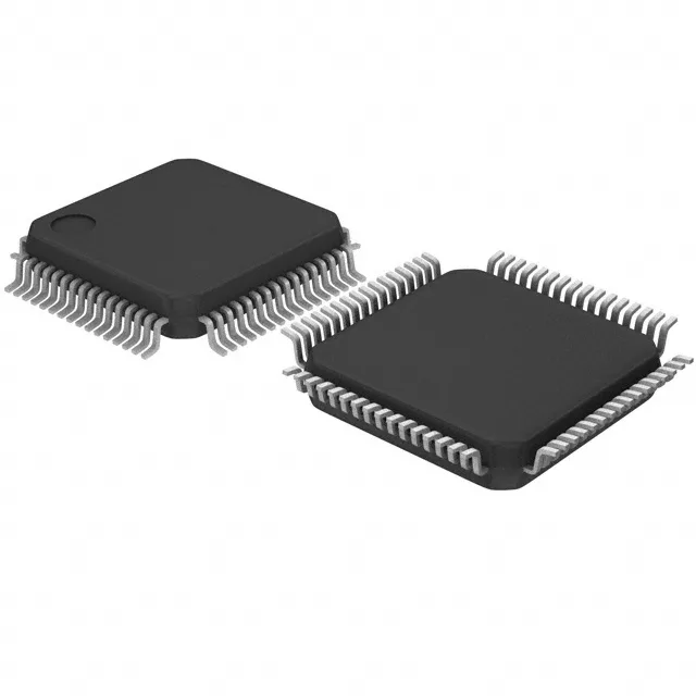
Package and footprint — 64-LQFP with 10x10 mm body
The 64-LQFP package (10x10 mm body, 0.5 mm pitch) is a common footprint shared with many STM32L4 and STM32F4 devices. That means a PCB layout designed for an STM32L476 or STM32F405 in the same package can often accept this part with only firmware changes.