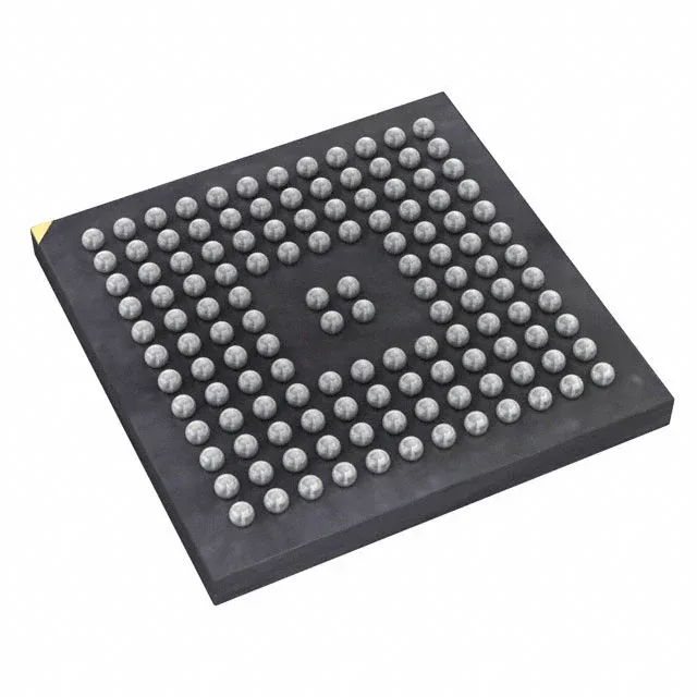
It packs 109 I/O lines and a rich peripheral set including CANbus, USB OTG, QSPI, multiple I²C and SPI interfaces, plus an integrated LCD driver — all in a 132-ball UFBGA (7x7 mm) package.
That 1.71 V floor is the same as the STM32L4's internal brown-out reset threshold, so you don't need an external supervisor for the low-voltage edge — the chip handles its own power-fail sequencing.
The base product number is STM32L476, so any PCN or EOL notice from ST would reference that family — keep an eye on the STM32L4 roadmap if you need a drop-in migration path to a higher-density or lower-power variant later.
132-UFBGA footprint — layout checklist
The 109 I/O count means most of the balls are assigned to GPIO and peripherals; the power and ground balls are distributed across the array, so the PCB stack-up must handle the current density. For rework, a hot-air station with a BGA nozzle and a pre-heater plate is mandatory — don't try this with a standard soldering iron.