80 MHz Cortex-M4 with FPU — sensor-fusion headroom in a WLCSP footprint
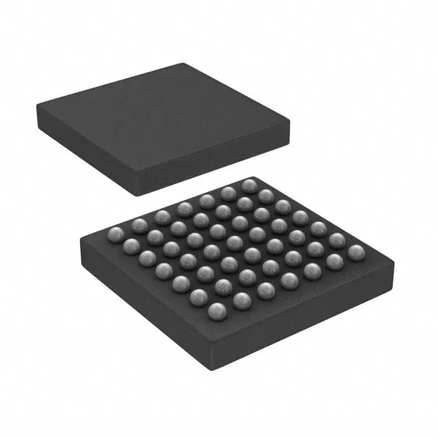
The STM32L443CCY6TR: Peripheral set includes CAN, USB, QSPI, SAI, and multiple I²C/SPI/UART channels. The 49-WLCSP package (3.14 x 3.13 mm) is the tightest footprint in the STM32L4 family.
256 KB Flash / 64 KB SRAM — sizing the firmware and OTA staging area
The 256 KB of Flash is split into 2 KB and 64 KB erase sectors. The 64 KB SRAM is single-cycle access at 80 MHz.
49-WLCSP — layout and reflow notes for the 3.14 x 3.13 mm package
The 49-ball WLCSP (0.4 mm pitch) demands a controlled reflow profile and a solder mask defined pad. The datasheet recommends a 0.25 mm diameter NSMD pad with a 0.3 mm solder mask opening. Keep the copper pour under the BGA area solid — no breakout traces between balls — and use a 0.1 mm stencil. The package is MSL 3; bake at 125 °C for 48 hours if the moisture barrier bag has been open longer than the floor life.
No end-of-life notification has been issued. For production planning, the base number STM32L443 covers multiple Flash and package variants.