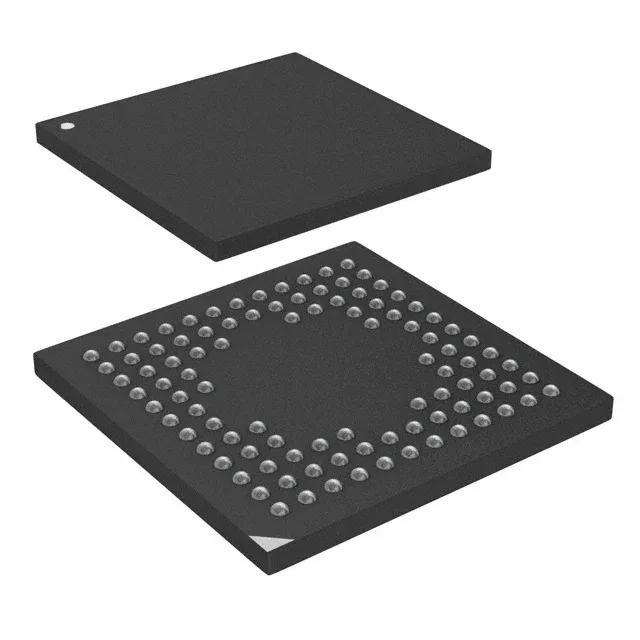
80 MHz Cortex-M4 with 256 KB Flash — sizing the firmware budget
The STM32L433VCI6: 83 I/O lines, CANbus, I²C, SPI, UART, USB, QSPI, LCD driver, 16-channel 12-bit ADC, and dual 12-bit DACs.
100-UFBGA (7x7) — footprint and reflow considerations
The fine pitch (0.5 mm typical) requires tight PCB registration and via-in-pad capability if routing escape traces under the body.
This removes the sourcing risk for new designs and production ramps. For dual-sourcing resilience, the STM32L4 family includes pin-compatible density variants (e.g., 512 KB Flash parts) that share the same 100-UFBGA footprint, though firmware migration and peripheral differences must be validated.
Peripheral set and connectivity — what hooks up where
Beyond the core, this MCU integrates a brown-out detect/reset, DMA controller, LCD driver, PWM timers, and a watchdog timer. Connectivity spans CANbus, I²C, IrDA, LINbus, MMC/SD, QSPI, SAI, SPI, SWPMI, and multiple UART/USART channels — enough to bridge sensors, displays, wireless modules, and fieldbus interfaces in a single chip.