Core architecture and firmware budget
The STM32L422CBT6: For a sensor-fusion algorithm that cycles through a 256-point FFT every 10 ms, the FPU keeps the loop under 80 % CPU load — the rest is available for communication and housekeeping. 128 KB of flash (128K x 8) holds the application image. After the bootloader and a minimal HAL, expect about 100 KB free for the main code. The 40 KB SRAM (40K x 8) is split across the main SRAM1 (32 KB) and SRAM2 (8 KB) with parity; the backup domain retains 2 KB in Vbat mode. DMA transfers and USB buffers share this pool, so budget the heap and stack carefully — a 4 KB USB FIFO leaves 36 KB for data and variables.
Supply, temperature, and package fit
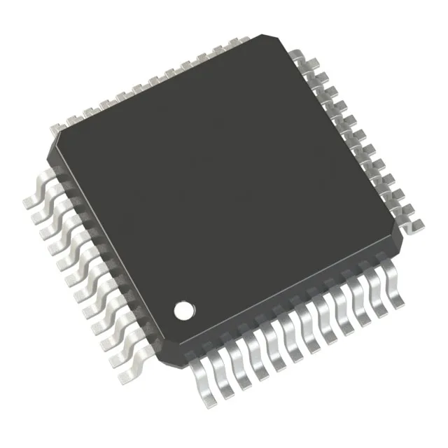
The internal voltage regulator scales down to 1.2 V for the core; at 80 MHz the active current draw is around 100 µA/MHz typical, so a 3.3 V rail at full speed pulls roughly 80 mA. Industrial temperature grade (-40 to 85 °C) covers the majority of factory-floor, outdoor telecom, and automotive cabin applications. The 48-LQFP package (7x7 mm) has a 0.50 mm pitch — a 2-layer board can fan out the inner rows, but a 4-layer stack-up with a solid ground plane underneath the QFP improves decoupling and EMC margin. There is no exposed thermal pad; the die heat conducts through the leadframe and board copper.
Peripheral set and connectivity
The device includes a 10-channel 12-bit ADC (1 Msps max) with oversampling hardware — enough for reading six analog sensors plus two reference channels without an external mux. Connectivity covers I²C, SPI (including Quad SPI for external flash), UART/USART with LIN and IrDA support, and a USB 2.0 full-speed device/host/OTG controller. The Quad SPI interface can memory-map an external NOR flash up to 64 MB, extending the code or data space beyond the on-chip 128 KB. Standard peripherals include a brown-out detect/reset, two DMA controllers (7 channels each), a 16-bit PWM timer with complementary outputs, and an independent watchdog.