On-chip peripherals include a 12-bit ADC with 16 channels, multiple I2C, SPI, and UART/USART interfaces, plus DMA and a PWM timer set — enough for sensor fusion, metering, and IoT edge-node control loops.
The 128 KB Flash is sized for moderate application code plus a bootloader, while the 20 KB SRAM handles stack and data buffers for real-time processing. The separate 6 KB EEPROM is a genuine on-chip EEPROM, not emulated Flash — it supports single-byte writes and the rated endurance of 100k cycles typical for the STM32L0 family, so calibration constants, configuration parameters, and data-logging counters survive power loss without external serial EEPROM or wear-leveling code.
Supply voltage and power rail design
The lower end is key for battery-powered designs where the cell voltage drops below 2 V; the upper end covers standard 3.3 V logic without a separate regulator.
Package and I/O count for board layout
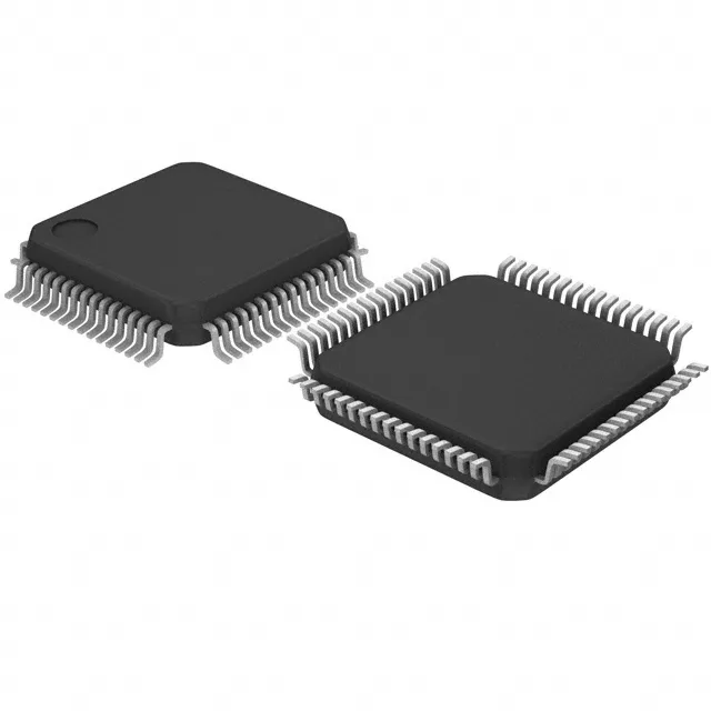
The 64-LQFP (10x10 mm) package with 51 I/O gives a good pin-to-area ratio for dense sensor arrays or parallel interfaces. The fine-pitch QFP is hand-solderable in rework but benefits from a solder-paste stencil for production. All I/O are 5 V-tolerant on the STM32L0 series, simplifying level translation when interfacing with legacy 5 V peripherals.