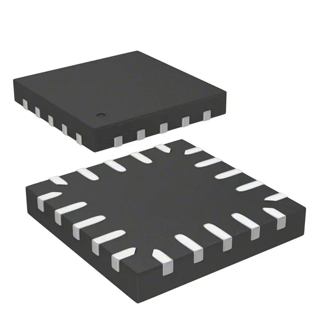
32 MHz Cortex-M0+ in a 3x3 mm package — the ultra-low-power endpoint MCU
The 20-UFQFPN package (3x3 mm) fits densely populated sensor PCBs and wearable form factors.
Memory sizing — the firmware ceiling and the EEPROM advantage
With 16 KB of Flash and 2 KB of SRAM, this MCU is sized for a single-purpose firmware image — a Modbus RTU slave, a temperature logger, a hall-sensor commutation loop, or a BLE-hub co-processor. The 512 bytes of on-chip EEPROM is a practical advantage: configuration parameters, calibration constants, and node addresses can be written byte-by-byte without wearing out a Flash sector or requiring an external serial EEPROM. The 7-channel 12-bit ADC covers multi-sensor analog front ends — thermistor, strain gauge, photodiode — on a single chip.
Active production — no end-of-life overhang
STMicroelectronics lists the STM32L011F4U3TR with a current product status and an Active lifecycle stage. The 20-UFQFPN package is a standard STM32L0 footprint, so if a future density upgrade is needed, the pin-compatible STM32L031 or STM32L051 variants share the same 3x3 mm land pattern — a clean board-spin path without a layout change.
The date-code trace and the 3x3 mm package reality
The UFQFPN package has an exposed thermal pad on the bottom — the 3x3 mm body means the pad is roughly 2.1 x 2.1 mm. A via-stitch pattern under the pad is not optional if the MCU draws more than 50 mA continuous at 125°C; the datasheet's thermal resistance figures assume a solid copper pour with at least four thermal vias. When inspecting incoming stock, the laser-etched marking on the top of the package should read 'STM32L011F4' in ST's standard font — any sanded or re-marked surface is a red flag. ST date-codes for this package are typically YWW with a two-letter plant code; a lot with inconsistent date-codes across a single reel should be X-rayed for die-bond integrity.