On-chip peripherals include a 12-bit ADC with 10 channels, DMA, a PWM timer, and a brown-out detect / POR block that simplifies power-on sequencing.
Package and board-fit realities
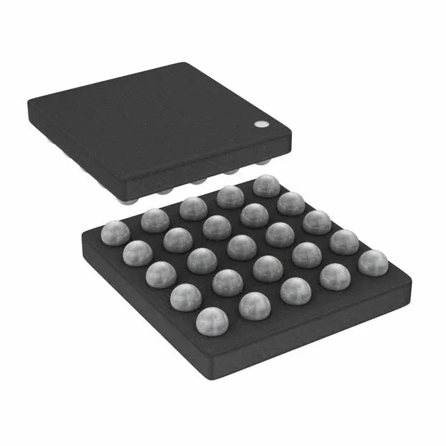
The part comes in a 25-ball WLCSP (wafer-level chip-scale package), supplier device package 25-WLCSP. That means the die is essentially the package — no plastic overmold, no leads. For a rework tech: WLCSP is not hand-solderable; you need a hot-air rework station with a fine nozzle and a preheat plate. The 21 I/O lines are accessible on the ball grid, so the PCB fan-out via pattern matters — expect micro-vias or via-in-pad if the board density is high.
That covers outdoor telecom cabinets, factory-floor sensors, and engine-bay-adjacent electronics that aren't directly on the block. Supply voltage down to 1.65 V means this MCU will keep running through a battery's full discharge curve — a real advantage in coin-cell or two-AA applications.
Memory and peripheral budget
16 KB Flash and 2 KB RAM is a tight fit. You are looking at a single-purpose firmware image — a bootloader plus one application, no OTA staging area unless you page the Flash in 1 KB sectors. The 512-byte EEPROM is useful for calibration constants or configuration that survives reprogramming. Connectivity is I2C, SPI, UART/USART, and IrDA — enough for a simple sensor hub or a serial bridge. The 10-channel 12-bit ADC samples at up to 1.14 Msps in the STM32L0 family, enough for audio-rate or low-speed data acquisition.
Sourcing and lifecycle position
The base product number is STM32L011, which spans several Flash and package options in the same die family.