480 MHz Cortex-M7 with 2 MB Flash — the firmware engineer's view
The STM32H742VIH6 packs 2 MB of Flash and 692 KB of RAM in a 100-ball TFBGA package. The 480 MHz core clock is the headline number, but the RAM split (ITCM, DTCM, AXI SRAM) is what determines whether your real-time buffers fit without spillover into slower AXI space. Keep the errata sheet handy for the flash prefetch and cache behaviour at this speed.
Peripheral set and connectivity — what the BOM gets
The part carries 82 I/Os, a 36-channel 16-bit ADC, and a dual 12-bit DAC. The internal oscillator is rated as the clock source, but for Ethernet or USB you will typically route an external crystal or oscillator to the HSE pins.
Package and temperature grade — board-level fit
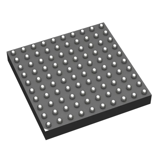
Housed in a 100-ball TFBGA (8x8 mm body), the STM32H742VIH6 is a surface-mount BGA. BGA rework needs a pre-bake if the moisture barrier is compromised; the 8x8 mm pitch is fine for a standard reflow profile. No underfill is required for normal shock and vibration, but a conformal coat over the assembly is advisable in condensing environments.
No official second source exists, but the STM32H7 family shares a common pinout across the 100-ball TFBGA density options, so a BOM-qualified alternate within the series is a pin-compatible swap if the firmware footprint fits.