170 MHz Cortex-M4F with FPU — where the speed matters
This combination targets real-time control applications such as field-oriented motor drives, digital power conversion, and industrial sensors where the math throughput and multi-channel acquisition close the loop without an external FPGA or companion ADC. The 170 MHz core with hardware FPU handles nested PI loops and Clarke/Park transforms in firmware, while the 12-bit ADC bank samples three-phase currents simultaneously. The four DAC outputs can serve as analog reference or feed a dither signal for high-resolution PWM. For a motor-control BOM, this MCU absorbs the sensor interface, the control algorithm, and the communication stack (CAN, UART, SPI) into one package.
Memory sizing for OTA and data logging
512 KB of Flash supports dual-bank firmware updates — one bank running the application while the other receives an OTA image. The 112 KB SRAM leaves room for a 64 KB ping-pong buffer for real-time data logging or a large FFT workspace without external memory.
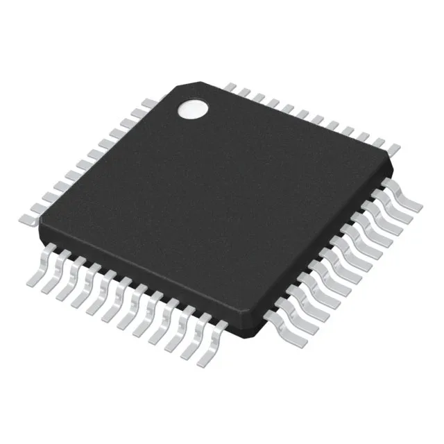
The LQFP package is hand-solderable for prototyping and reflow-friendly for production. No exposed pad on this package — thermal dissipation goes through the leads, so keep the ambient airflow adequate if running the core and ADC at full speed continuously.
STMicroelectronics lists the STM32G491CET6 as Active. This part is qualified for ongoing production and new design-ins.