170 MHz Cortex-M4 with math accelerators for mixed-signal control
The 42-channel 12-bit ADC bank and seven 12-bit DACs let it sample multiple current/voltage phases and output analog references simultaneously, reducing external component count in a mixed-signal BOM.
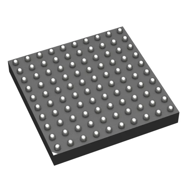
100-TFBGA (8x8 mm) — footprint and routing
Housed in a 100-ball TFBGA measuring 8x8 mm, this part is suited for space-constrained PCBs where a larger LQFP would not fit. The 86 available I/Os route to the ball grid; the fine-pitch BGA demands a controlled-impedance stackup and X-ray inspection for reflow quality.
The base number STM32G473 spans multiple density and package variants, so a future migration within the family — to a higher Flash or a different package — stays pin-compatible across the same G4 platform without a full board re-spin.
On-chip connectivity includes CANbus, I²C, SPI, UART/USART, USB, QSPI, SAI, and IrDA — enough for a gateway node aggregating sensor buses and a display link. The internal oscillator and brown-out/POR/WDT reduce external clock and supervisor ICs. DMA offloads ADC result transfers and UART data movement without core intervention, preserving the 170 MHz cycles for control math.