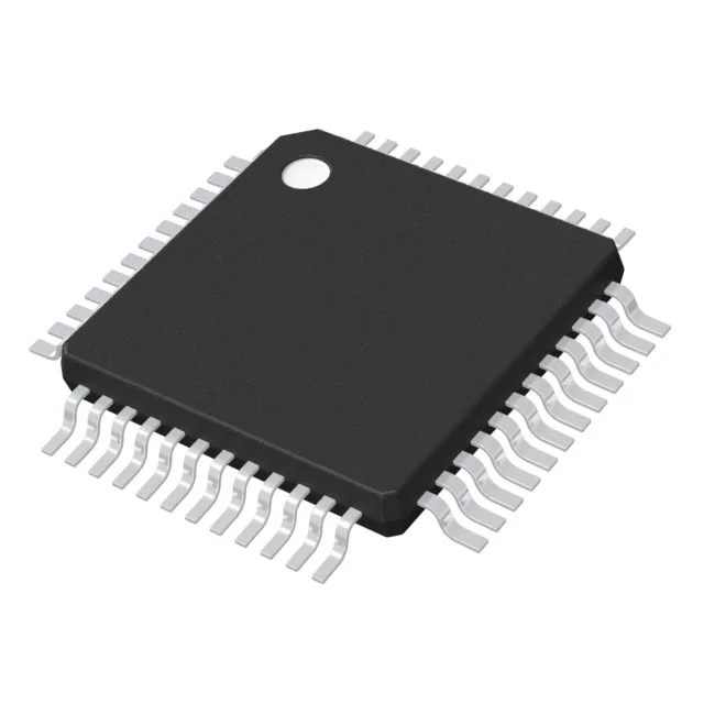
Housed in a 48-LQFP package with 44 I/Os, it targets cost-sensitive control applications such as sensor nodes, motor control, and simple human-machine interfaces.
The 8 KB SRAM limits runtime data buffers; designs that need larger packet buffers or multiple concurrent tasks should verify headroom early. The Flash is organized as 16 KB x 8 bits, and the part supports in-application programming via the built-in bootloader.
This simplifies the power architecture in portable and low-power designs.
No extended-temperature variant is needed for these applications, keeping the BOM cost down.
For dual-sourcing or higher-density requirements, the STM32G0 family includes pin-compatible variants with larger Flash and RAM — the base product number is STM32G031, and the family shares the same 48-LQFP footprint across density options.