216 MHz Cortex-M7 — what the speed rating means for your pipeline
The STM32F779AIY6TR runs an ARM Cortex-M7 core at 216 MHz — this is the maximum clock from the internal PLL, not a burst turbo. At this frequency the core delivers roughly 1080 CoreMark / 462 DMIPS, limited by the flash wait-state profile at zero wait states up to the ART Accelerator ceiling. For a real-time control loop or an audio processing chain, the 216 MHz ceiling sets the interrupt latency floor and the FFT bin count you can sustain without stalling on prefetch. The 2 MB on-chip flash and 512 KB SRAM give enough headroom for a dual-bank firmware update scheme — one bank running the application, the other receiving the new image over USB OTG or Ethernet without external memory. The 512 KB SRAM is split across 256 KB of general-purpose RAM plus 128 KB of DTCM and 64 KB of ITCM — the TCM regions run at core clock with zero wait states, so time-critical interrupt vectors and stack can live there.
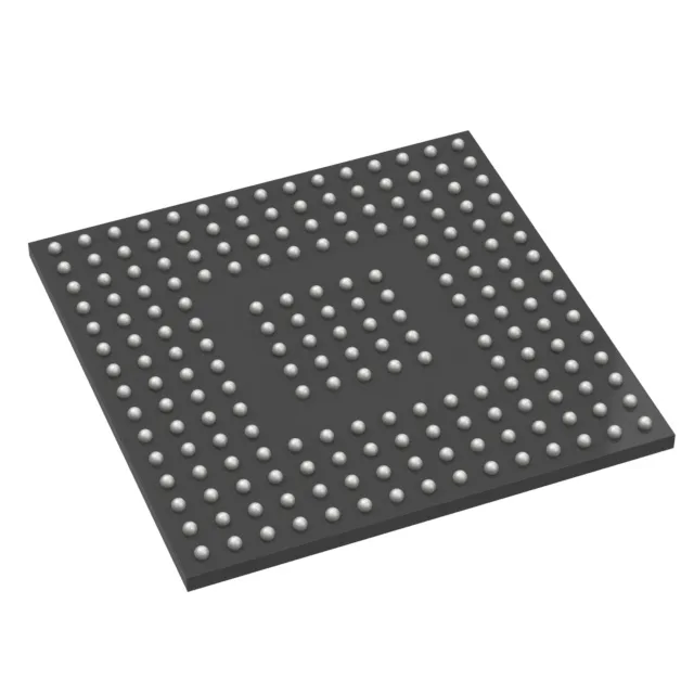
180-WLCSP — board-level implications of the package choice
This part ships in a 180-ball WLCSP (Wafer-Level Chip-Scale Package) measuring 5.5 x 6.0 mm — the die itself is the package, with solder balls directly on the die pads. There is no molded body and no exposed thermal pad. The 0.4 mm ball pitch demands a high-density PCB with microvias and blind/buried vias for fan-out; a standard 4-layer board with through-hole vias will not route all 129 I/O plus the power and ground balls. Plan for at least an 8-layer stack-up with laser-drilled microvias in the BGA escape region. Thermal dissipation is through the solder balls into the PCB copper — no metal pad to solder to. The junction-to-board thermal resistance (RθJB) is higher than a QFP or LQFP equivalent, so the STM32F779AIY6TR suits applications where the MCU draws under 300 mW continuous and the board has a solid ground plane. For higher power dissipation, consider the LQFP176 or BGA176 package variants in the same STM32F7 family.
Connectivity and peripherals — display and camera interface onboard
The STM32F779 integrates a TFT LCD controller supporting up to XGA resolution (1024x768) with an 8-bit parallel interface, plus a camera interface for a parallel video sensor. Combined with the Chrom-ART graphic accelerator (DMA2D), this MCU can drive a display and composite camera frames without burdening the Cortex-M7 core — useful for an HMI panel that shows live video preview alongside touch controls. Connectivity includes dual CAN 2.0B, USB OTG HS/FS with on-chip PHY, Ethernet MAC with dedicated DMA, and multiple I²S/SAI audio interfaces — enough to serve as the application processor in a building automation gateway or an audio effects pedal. The 129 GPIOs, many with 5 V tolerance, reduce the need for external level shifters when interfacing to legacy 5 V logic or sensor buses.
RoHS3 compliant (2011/65/EU + 2015/863) with no exemptions — the WLCSP package uses lead-free solder balls and halogen-free mold compound. No REACH SVHC declarations beyond the standard semiconductor bill of materials; compliance documentation is available upon request.