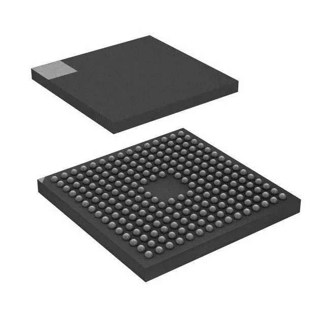
It packs 2 MB of Flash and 512K x 8 of SRAM, giving firmware teams room for complex protocol stacks, OTA update staging, or frame buffers without external memory. The 159 I/O lines in a 216-TFBGA package (13x13 mm) allow dense peripheral integration on a compact board — useful for HMI panels or multi-axis drives where every pin counts.
Combined with the 512K x 8 SRAM, you can hold a sizeable data buffer for encoder feedback or waveform synthesis without cache-thrashing. The 2 MB Flash supports in-application programming via the built-in bootloader, so field firmware updates over Ethernet or CAN are practical.
Package and footprint — 216-TFBGA
The 159 GPIOs fan out to the outer balls, making layout feasible on a 4-layer board with careful via fanout.