It targets applications that need a high-performance compute core and rich peripheral set in the smallest possible footprint — think advanced human-machine interfaces with LCD, real-time audio processing over SAI or SPDIF, and industrial communication stacks running CAN, USB OTG, or Ethernet over the external bus interface.
With 2 MB of program Flash and 512 KB of SRAM, this MCU sits at the high end of the STM32F7 value line. The Flash is enough for a full GUI stack with a graphics library plus a real-time OS kernel and application code. The 512 KB SRAM handles multiple frame buffers for a WQVGA display or large audio sample buffers without needing external memory. For designs that push beyond 512 KB of working memory, the EBI/EMI and QSPI interfaces let you attach SDRAM or serial NOR Flash externally, but the internal RAM covers most single-chip scenarios.
WLCSP package — footprint and assembly considerations
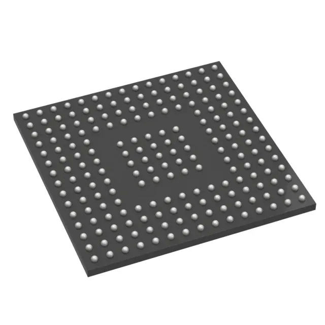
The 180-ball WLCSP (5.5×6 mm) is the tightest package option for this part. It saves board area versus a 176-pin LQFP but demands a controlled assembly process: the 0.4 mm ball pitch needs a solder mask defined pad with a microvia-capable PCB stackup. The package is not intended for hand-soldering or rework without a BGA rework station.