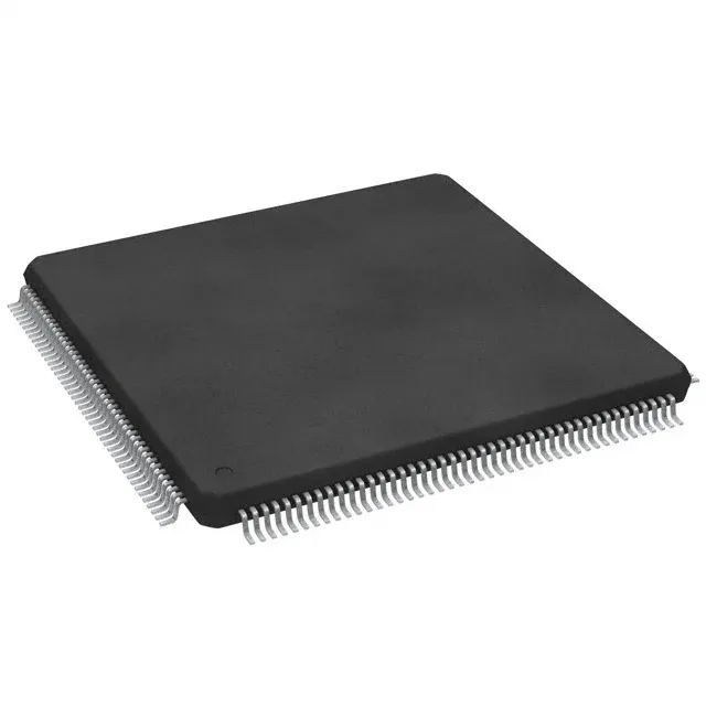
ARM Cortex-M7 at 216 MHz — the performance tier for signal processing and HMI
The STM32F767IIT6: It targets applications that need real-time DSP throughput, rich connectivity, and a wide I/O count — think industrial motor drives with Ethernet, HMI panels with LCD and touch, or IoT gateways juggling CAN, USB OTG, and multiple UARTs. The Cortex-M7 core includes a single-precision FPU and a 6-stage pipeline, so FFTs, filter loops, and control-law calculations run without a separate DSP. The 140 I/O pins give you room to mux in parallel buses (EBI/EMI for external SRAM or NOR Flash), a camera interface, and multiple SPI/I²C peripherals without starving the display or the sensor array. The 12-bit ADC bank has 24 channels, enough for multi-phase current sensing or a dozen analog inputs.
216 MHz — clock-tree setup and flash wait states
The 216 MHz PLL output needs the ART Accelerator™ enabled and the flash wait states set to at least 7 cycles at 3.3 V, or the core hard-faults on the first branch. The internal oscillator (HSI) runs at 16 MHz, so the bootloader and first-power code should configure the PLL before enabling the prefetch buffer. SWD debug stays alive even with the watchdog armed, which saves a production-line headache.
2 MB Flash and 512 KB SRAM — firmware and buffer budget
2 MB of Flash lets you hold a full TCP/IP stack, a graphics library, and a FAT filesystem with room for OTA staging. The 512 KB SRAM splits into 240 KB of DTCM (tightly coupled for deterministic data access) and the rest as general-purpose SRAM — the DTCM region is what the Cortex-M7 uses for zero-wait-state data, so put your interrupt stacks and audio buffers there. Quad-SPI memory-mapped mode can expand the code space without touching the internal Flash.