The 216 MHz core with its single-cycle multiply-accumulate and double-precision FPU handles sensor fusion and motor-control FOC loops in software, skipping a dedicated DSP or FPGA. The 2 MB Flash is split into 1 MB banks with 128-bit read width, so the CPU fetches instructions without wait states at 216 MHz as long as ART Accelerator prefetch is enabled. The 512 KB SRAM is organised as 368 KB of general-purpose RAM plus 128 KB of DTCM (tightly coupled data memory) and 16 KB of ITCM — the DTCM is where you put the interrupt stacks and real-time data arrays to avoid bus contention. The internal oscillator trims to 1 % accuracy, so a crystal is optional for non-timing-critical UART or CAN applications — saves a BOM line and board area.
Package reality — BGA rework, not a field swap
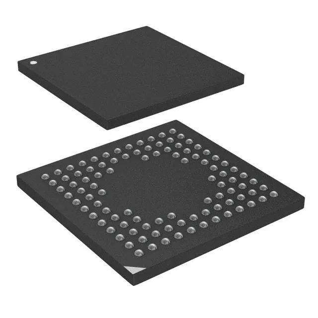
This is a 100-ball TFBGA in an 8x8 mm array with 0.5 mm pitch. No lab, no bench, let us go — except this part does not go in the field kit. The BGA needs X-ray inspection after reflow, and rework requires a hot-air station with a preheater and a stencil for the solder paste. The 0.5 mm pitch means the PCB fab needs via-in-pad or microvias to route the inner balls out. The thermal pad is on the bottom; a via stitch under the package to the ground plane is mandatory if the part dissipates more than 300 mW continuous. MSL 3 out of the bag — if the moisture-barrier bag has been open longer than the floor-life window, bake the trays at 125 °C for 48 hours before reflow.
The on-chip brown-out detect and POR keep the core from running wild during a cold-crank or a brown-out event.