STMicroelectronics STM32F765NIH6TR — Microcontrollers & Processors (MCU / MPU / DSP)

STM32F765NIH6TR ARM Cortex-M7 MCU, 216 MHz, 2 MB Flash

MPNSTM32F765NIH6TR
Active

STMicroelectronics STM32F7 series STM32F765NIH6TR, ARM Cortex-M7, 32-Bit Single-Core MCU, 216MHz, 2MB Flash, 512K x 8 RAM, 216-TFBGA, -40°C~85°C.

$16.3709Ref. price · indicative, final on quote
Independent supplier — new & surplus stockAuthenticity-screened · ESD-safe packingListing updated Jul 2026

Specifications

STM32F765NIH6TR specifications
ParameterValue
SeriesSTM32F7
MountingSurface Mount
Oscillator typeInternal
Program memory typeFLASH
Voltage - supply (Vcc (Vdd))1.7V ~ 3.6V
Operating temperature-40°C~85°C(TA)
Speed216MHz
PackageTape & Reel (TR)
RAM size512K x 8
Core size32-Bit Single-Core
PeripheralsBrown-out Detect/Reset, DMA, I²S, POR, PWM, WDT
ConnectivityCANbus, EBI/EMI, Ethernet, I²C, IrDA, LINbus, MMC/SD/SDIO, QSPI, SAI, SPDIF, SPI, UART/USART, USB OTG
Number of i (O)168
Core processorARM® Cortex®-M7
Case216-TFBGA
Data convertersA/D 24x12b; D/A 2x12b
Program memory size2MB (2M x 8)

Product details

It sits in the STM32F7 series, targeting applications that need a balance of DSP throughput and peripheral integration — think motor drives, industrial Ethernet nodes, and multi-protocol gateways. The 216 MHz core clock gives it enough headroom for real-time control loops and audio processing without an external DSP. The 2 MB Flash can hold a full application plus an OTA staging area, and the 512K RAM supports multiple protocol stacks or a framebuffer for a small GUI. No last-time-buy or obsolescence risk to factor into your BOM planning.

216-TFBGA — what the package means for the board and rework

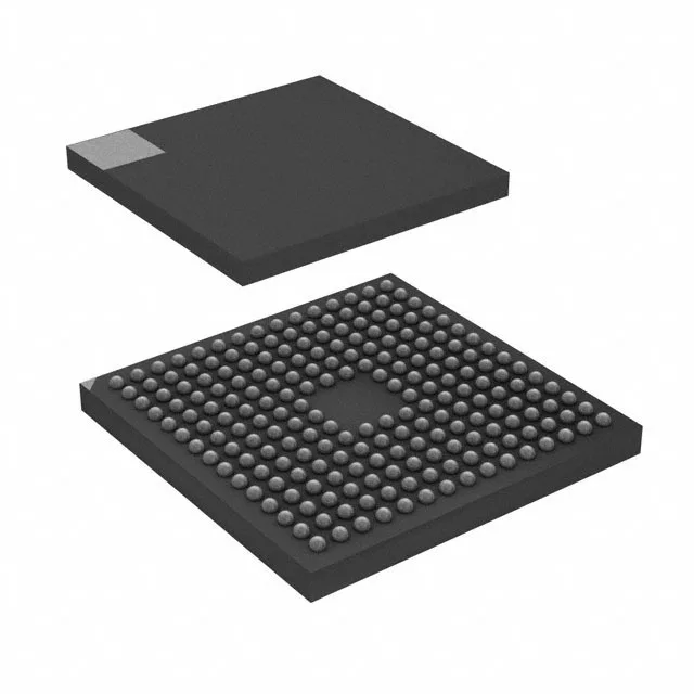
The STM32F765NIH6TR comes in a 216-ball TFBGA (Thin Fine-Pitch Ball Grid Array) measuring 13x13 mm. That's a dense, fine-pitch BGA — not something you hand-solder with a hot-air station unless you have a stencil and a reflow profile dialled in. The 0.8 mm ball pitch is forgiving enough for a four-layer board with via-in-pad if you tent the vias, but the 13x13 array means routing all 168 I/O out requires at least four signal layers. Expect to use microvias or blind vias on the inner rows. The TFBGA variant is thinner than a standard FBGA, which helps in height-constrained enclosures but means the package has less thermal mass — the exposed die sees the reflow profile faster, so watch the ramp rate.

Peripheral set — what connects where

The 168 I/O give enough headroom to wire up a parallel LCD, an external memory bus via EBI/EMI, and still have pins left for sensors and actuators. Internal oscillator is included, so a basic blink or UART test doesn't need an external crystal. For Ethernet or CAN with tight timing, you'll still want an external oscillator — the internal RC is ±1% accuracy, enough for boot but not for a 100 Mbps PHY.

Frequently asked questions

Can STM32F765NIH6TR replace STM32F767NIH6?

The STM32F765NIH6TR and STM32F767NIH6 share the same base package and pin count (216-TFBGA), but the STM32F767 adds a hardware JPEG codec and a few additional peripherals. If your application doesn't need the JPEG accelerator or the extra features, the STM32F765 is a drop-in replacement at the same pinout. Verify the firmware peripheral configuration — the register maps are nearly identical, but the F767 has additional memory-mapped blocks that the F765 lacks.

What is the core architecture and maximum frequency of STM32F765NIH6TR?

The core is an ARM Cortex-M7, 32-bit single-core, running at a maximum clock speed of 216 MHz. This is the highest frequency tier in the STM32F7 series without the Chrom-ART graphics accelerator.