216 MHz Cortex-M7 with 1 MB Flash — the memory-and-throughput tier
The 1 MB Flash and 512 KB SRAM support firmware images with embedded GUI stacks, Ethernet TCP/IP offload, or dual-precision DSP routines, while the 168 general-purpose I/O give board-level integration flexibility for parallel buses and sensor arrays.
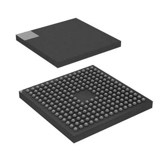
216-TFBGA — what the BGA footprint means for the board
Not a hand-solder or rework-friendly package — plan for X-ray inspection and a reflow profile matched to the solder-ball alloy. The 168 I/O are distributed across the ball map, so signal routing needs careful pin assignment early in the layout phase.
Connectivity and peripheral set — what is on-chip
This peripheral density eliminates the need for external bridge chips in many designs — a single MCU handles the control, display, and wired-connectivity stack.
This makes it a safe selection for new designs and production ramps. The base product number is STM32F765, so the same BOM can scale across Flash and package variants within that family without requalifying the entire firmware.