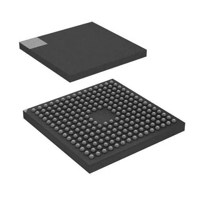
The STM32F746NGH6TR: That core clock is the headline number for this part: it puts the F746 in the performance tier for the STM32F7 family, capable of handling real-time control loops, graphics pipelines, and protocol stacks without breaking a sweat. The 168 GPIOs and rich peripheral set — Ethernet MAC, CAN 2.0, USB OTG HS, multiple SPI/I²C/UART, plus a 24-channel 12-bit ADC and a 2-channel 12-bit DAC — mean this chip can sit at the center of a complex embedded system without needing external bridges or memory expansion for most designs.
Industrial temperature range and BGA package — field-fit considerations
The 216-ball TFBGA (13×13 mm) is a fine-pitch BGA — not a field-swap part. On-site replacement means hot air or a rework station, and the board needs X-ray inspection afterward.
Supply range and power-up sequence
At 1.7 V the 216 MHz PLL may not lock cleanly — the datasheet's operating conditions table is the authority for minimum VDD at full speed. The part includes brown-out detect and POR, so external reset supervision is optional for most designs. Internal oscillator is present, but for Ethernet or USB operation an external 25 MHz crystal is the usual choice for clock accuracy.
For BOM planning, the base product number STM32F746 covers multiple Flash and package variants within the same family, so a pin-compatible drop-in with different memory density is possible if the application requirements shift.