1 MB Flash / 384 KB RAM — sizing the BOM
The 1 MB Flash (organized as 1M x 8) and 384 KB SRAM (384K x 8) define the firmware and data budget. For a 480x272 TFT with a 16-bit colour frame buffer, the display buffer alone consumes about 260 KB, leaving 124 KB for stack, heap, and peripheral DMA buffers. The Flash is sufficient for a FreeRTOS application with a LwIP stack, FATFS file system, and a touchscreen driver — no external NOR or NAND needed for most mid-complexity HMI projects. If the application grows beyond this, stepping to the STM32F469NIH6 (2 MB Flash / 384 KB RAM) is the natural move.
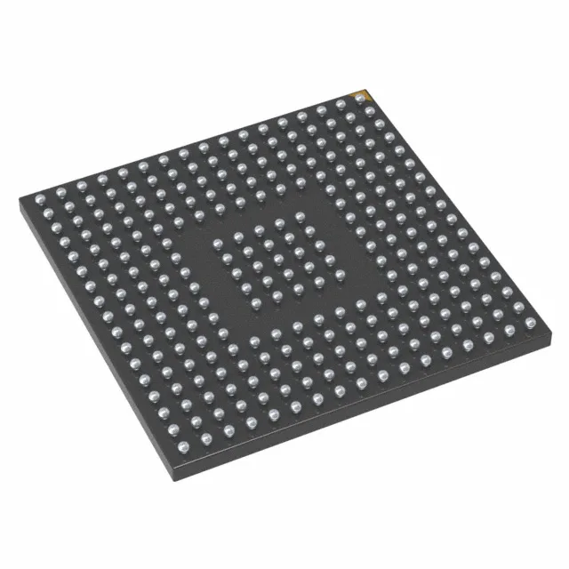
176+25 UFBGA (10x10 mm) — layout and rework
That pitch demands a controlled-impedance PCB stackup with microvias or blind vias for breakout — four-layer boards are typical, six-layer if the Ethernet PHY and external memory bus are routed. MSL 3 out of the bag — bake at 125°C for 48 hours if the moisture barrier bag has been open longer than the floor-life window.
For a production BOM this means no immediate obsolescence risk, though the usual PCN monitoring for package or wafer-fab changes applies — ST typically gives a 6- to 12-month transition window on any process change.