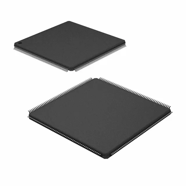
Device overview: STM32F439BGT6
It runs at 180 MHz and packs 1 MB of Flash and 256 KB of SRAM.
Memory and bus: 1 MB Flash, 256 KB SRAM, 180 MHz core
The 180 MHz core clock is the highest in the STM32F4 value-line; you will need to configure flash wait states (typically 5 cycles) before raising the system clock past 120 MHz or the first instruction fetch hard-faults. The 1 MB Flash supports a single OTA staging area if you reserve a sector for the bootloader. The 256 KB SRAM is split across multiple blocks — the 64 KB CCM (core-coupled memory) is not DMA-accessible, so route time-critical interrupt vectors there for zero-wait execution.
Connectivity and peripherals: Ethernet, USB OTG, CAN
The integrated Ethernet MAC works with an external PHY via the RMII interface — the MAC itself is IEEE 1588 capable, useful for precision time-stamping in industrial control. USB OTG FS/HS requires an external PHY for high-speed operation; the on-chip FS PHY handles device and host modes at 12 Mbps. Two CAN 2.0B interfaces are present for automotive or industrial bus networks. The EBI/EMI supports parallel NOR/NAND Flash and SRAM, which can offload the internal memory for large frame buffers.
Decouple each VDD pair with a 100 nF ceramic plus a 4.7 µF bulk per bank.
For BOM planning, the base product number STM32F439 covers multiple density and package variants — verify the specific suffix (BGT6 for 208-LQFP, tray) when ordering.