180 MHz Cortex-M4 in a WLCSP — what that means for a board bring-up
It packs 114 I/O lines, a rich peripheral set including Ethernet MAC, CAN 2.0B, USB OTG, and an external memory interface (EBI/EMI), plus dual 12-bit DACs and a 24-channel 12-bit ADC. This is the part you pick when you need a high-performance MCU with graphics or connectivity in the smallest possible footprint — think compact HMI panels, portable instrumentation, or fieldbus gateways that have to fit inside a DIN-rail housing.
WLCSP package — rework and layout realities
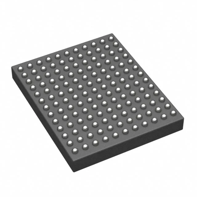
The 143-ball WLCSP (4.52 x 5.55 mm) is a wafer-level chip-scale package — no mould compound, the die backside is exposed. That means the package is essentially the size of the die itself, which saves board area but makes handling and rework more demanding. The ball pitch is fine enough that you will want a proper solder-paste stencil and a reflow oven with good profile control. No lab, no bench — if you are swapping this on site, you will need a hot-air station and a steady hand. The exposed die surface also means the part is sensitive to mechanical stress; avoid placing it near board flex points or under heavy components.
Connectivity and memory — what the peripheral set enables
The Ethernet MAC with dedicated DMA and the external bus interface (EBI/EMI) are the standout features here. The EBI/EMI lets you attach external SRAM, NOR Flash, or an LCD controller directly — no FPGA needed for a simple frame buffer. The Ethernet MAC supports MII/RMII, so you can add a PHY and run a real-time industrial protocol stack (EtherCAT, PROFINET, Modbus TCP) without an external communication co-processor. The 256K x 8 SRAM is enough for moderate data buffers and RTOS tasks, but if you are doing heavy graphics or packet buffering, plan on using the EBI/EMI to add external SDRAM or SRAM.