180 MHz Cortex-M4 with FPU — the compute tier this BOM sits at
The part is built for mid-to-high-complexity embedded control — think graphical HMI panels, motor-control PLCs, or industrial Ethernet gateways where the LCD controller and dual CAN interfaces earn their keep.
Running the core at 180 MHz from the internal oscillator or an external crystal means the flash wait state count needs bumping to at least 1 before raising the core clock past around 30 MHz, or the first branch instruction hard-faults. The PLL can be fed from the HSI or HSE; the 180 MHz ceiling is the SYSCLK limit, not the APB1/APB2 bus speeds, which are prescaled down from the AHB clock. The 256 KB SRAM is split across up to four memory blocks — the DTCM and ITCM regions give single-cycle access for time-critical interrupt handlers.
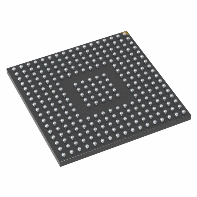
201-UFBGA — what the package drives on the board
The 201-UFBGA (176+25 UFBGA 10x10 mm) is a fine-pitch BGA with 0.5 mm ball pitch. That ball pitch forces at least a 4-layer PCB with microvias or via-in-pad for fanout on the inner rows — a 2-layer board will struggle to route the 140 I/O plus the Ethernet PHY interface and the FMC bus for external memory. The 10x10 mm body keeps the footprint compact, but the rework profile needs a preheat soak to avoid cold joints on the center balls.
For a production BOM that already qualifies this package variant, there is no urgency to requalify a second source — though the STM32F429IET6 (same package, larger Flash) is pin-compatible if the firmware image outgrows the 512 KB allocation.