That core speed, paired with 2 MB of Flash and 256 KB of SRAM, handles real-time control loops, sensor fusion, and communications protocol stacks without external memory.
Memory sizing — 2 MB Flash, 256 KB SRAM
The 2 MB Flash (2M x 8) and 256 KB SRAM (256K x 8) give this MCU enough headroom for a full-featured RTOS, TCP/IP stack with TLS, and a modest file system. The Flash density supports over-the-air update staging with a backup image, while the SRAM covers packet buffers and control data. For designs that need more scratchpad, the EBI/EMI interface can connect external SRAM or NOR Flash without a glue-logic FPGA.
Peripheral set — Ethernet, CAN, and analog
Built-in Ethernet MAC and CANbus controllers eliminate the need for external PHY-management MCUs or CAN transceiver controllers, reducing BOM count and board area.
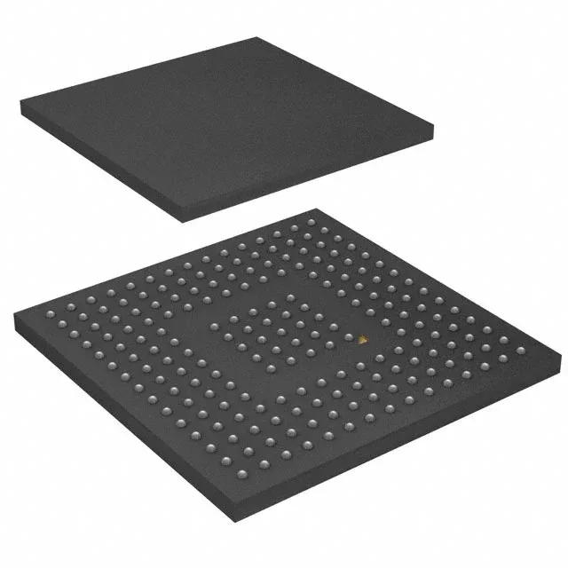
Package and layout — 176-UFBGA (10x10)
That compact footprint saves significant board area versus a 144-pin LQFP, but requires a multi-layer PCB with via-in-pad or microvias for fan-out. The BGA also demands a stencil and reflow oven — not hand-solderable.
For dual-sourcing resilience, ST's STM32F4 family includes pin-compatible density variants — the STM32F429 adds a TFT LCD controller and the STM32F437 adds a cryptographic accelerator — but the STM32F427IIH7 itself is not cross-referenced to a second-source vendor.