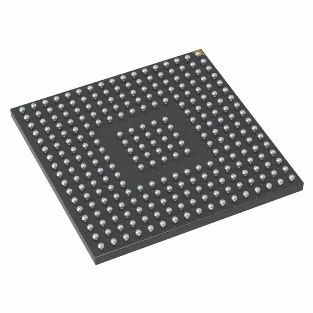
The STM32F427IIH6TR: The 176+25 UFBGA (10x10 mm) package brings 140 I/O lines and a peripheral set: dual CAN, Ethernet MAC, USB OTG, SPI, I2C, UART, and a 24-channel 12-bit ADC plus two 12-bit DACs.
The 176+25 UFBGA (10x10 mm) is a fine-pitch BGA with a 0.5 mm ball pitch. That means via-in-pad or microvias on the inner rows unless you route all signals on the top layer — plan for a four-layer board minimum. The package has no exposed thermal pad; heat dissipates through the BGA balls and the PCB copper. Under a hot-air station, pre-bake the board at 125°C for 8 hours if the reel has been open past MSL 3 floor life. Reballing is possible with a stencil and 0.3 mm solder spheres, but the 0.5 mm pitch leaves little room for misalignment — a rework station with split optics is the safe call.
Active lifecycle — no end-of-life concern on this line item
What the 180 MHz and 2 MB Flash mean for firmware and system architecture
The 2 MB Flash is organised as 1 MB dual-bank, which allows live firmware updates — write to one bank while executing from the other. The 256 KB SRAM is split into 128 KB of main SRAM plus 64 KB of CCM (core-coupled memory) and 64 KB of backup SRAM; the CCM gives zero-wait access for time-critical interrupt handlers. The 140 I/O lines, combined with the connectivity set (Ethernet, CAN, USB OTG, multiple SPI/I2C), mean this MCU can serve as the central controller in a distributed industrial system, handling both fieldbus communication and local sensor acquisition.