The 1 MB Flash and 256 KB SRAM leave room for a real-time OS, communications stacks, and moderate data buffering without external memory.
1 MB Flash / 256 KB SRAM — sizing the firmware and data budget
Program memory is 1 MB of Flash, organised as 1M x 8 bits. The 256 KB SRAM (256K x 8) is split across core RAM, backup SRAM, and CCM (core-coupled memory) — the CCM region gives zero-wait access for time-critical interrupt handlers or DSP coefficient tables. For designs that log data or run a TCP/IP stack with large buffers, the 256 KB SRAM is adequate; if you need more, the FSMC can map external SRAM, NOR Flash, or LCD controllers.
Industrial temperature range and BGA footprint
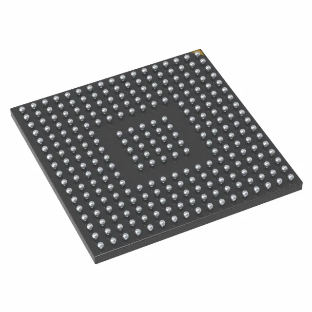
The 176+25 UFBGA package (10x10 mm body) packs 201 balls with a 0.5 mm pitch — expect a 4- or 6-layer PCB with microvias to route the peripheral signals.
STMicroelectronics lists the STM32F427IGH7 as Active (current product). ST's typical PCN lead time for STM32F4 series changes is 6–12 months, so the supply risk is low. If you need a second-source conversation, the STM32F427IGH6 (same die, different package variant) is the closest cross-ship — but verify the package compatibility with your board.