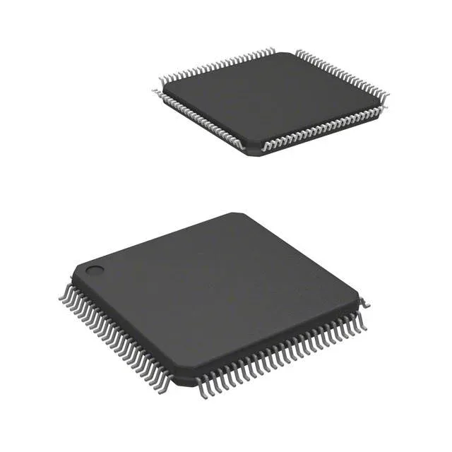
168 MHz Cortex-M4 with Ethernet — the industrial gateway processor
Its 1 MB on-chip Flash and 192K x 8 SRAM give firmware room for a full Ethernet stack, a CANopen node, and a USB OTG host stack simultaneously — the kind of memory partition that keeps the application code, communication buffers, and OTA staging area from competing for space. Connectivity is the headline differentiator here: Ethernet MAC with dedicated DMA, CANbus, USB OTG HS/FS, plus SPI, I²C, UART, and an 8-bit parallel camera interface (DCMI). That peripheral set maps directly to industrial gateway designs, edge controllers, and multi-protocol bridge nodes where the MCU must talk to a PLC over Ethernet, log data to USB storage, and poll a sensor bus over CAN — all without an external communication co-processor. The 100-LQFP package exposes 82 I/O, enough for an external memory bus (EBI/EMI) plus a parallel LCD interface and the full complement of serial peripherals.
Active lifecycle — no LTB horizon on this BOM line
For a procurement team qualifying a new design, this removes the single-source obsolescence risk that haunts older STM32F1 and F2 series parts. Design it into a five-year production run with confidence that the supply channel will remain open.
1 MB Flash and 168 MHz — sizing the firmware budget
The 1 MB Flash (1M x 8) is organized as twelve 16-KB sectors plus four 128-KB sectors — the dual-bank architecture supports live firmware updates via the built-in bootloader or a custom OTA agent. The 192K x 8 SRAM splits into 128 KB of general-purpose RAM, 64 KB of core-coupled RAM (CCM) accessible only by the CPU at full speed, and a 4-KB backup domain. The CCM is where interrupt service routines and time-critical control loops live without competing with the DMA traffic on the main AHB bus. At 168 MHz, the Cortex-M4 executes one 16-bit DSP MAC per cycle, and the ART Accelerator prefetches Flash instructions to eliminate wait states for most code. The 16-channel, 12-bit ADC samples at up to 2.4 MSPS — fast enough for motor phase-current sensing or power-line monitoring with oversampling.
100-LQFP footprint and reflow considerations
The 100-LQFP package (14 mm × 14 mm, 0.5 mm pitch) is a standard JEDEC footprint with an exposed pad on the underside for thermal dissipation. MSL 3 handling applies: bake at 125°C for 8 hours if the moisture-barrier bag has been open longer than the floor-life window before reflow. Decoupling: one 100 nF ceramic per VDD pair plus a 4.7 µF bulk cap on each supply rail. The VDDA analog supply needs an LC filter if the ADC or DAC is used at full resolution — a ferrite bead plus 10 µF / 100 nF pair is standard practice from ST's application note on the F4 series.