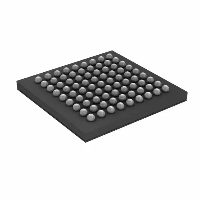
Selection note: 100 MHz Cortex-M4 in a WLCSP footprint
The STM32F413MGY6TR uses an 81-WLCSP package (4.04 x 3.95 mm), the smallest footprint in the STM32F413 line, suited for space-constrained PCBs.
Memory and throughput: what the 1 MB / 320 KB / 100 MHz combination buys you
The 1 MB Flash is sized for a full application stack including a TCP/IP or USB host stack; the 320 KB SRAM avoids external memory in most designs, though the EBI/EMI interface is there if you need it.
WLCSP package: board-level implications
This gives the smallest footprint but requires a controlled SMT process: the solder balls are directly on the die pads, so board-level reliability depends on the PCB's coefficient of thermal expansion matching the silicon. Use a solder mask defined pad with the recommended NSMD (non-solder mask defined) layout from the STM32F413 application note.
This is a standard STM32F4 part, not a niche or legacy variant, so allocation risk is lower than for older or less common order codes. For dual-sourcing resilience, the STM32F413 family includes multiple density and package options sharing the same core and peripheral IP, but the WLCSP footprint is specific to this package variant — a pin-compatible second source within the STM32F4 series does not exist from another manufacturer.