It packs 114 I/O lines, a rich peripheral set including CANbus, USB OTG, QSPI, and multiple UART/SPI/I²C interfaces, plus a 16-channel 12-bit ADC.
The 1 MB Flash is enough for a full application stack plus OTA staging buffer; the 256 KB SRAM supports moderate frame buffers or communication packet queues. If your firmware footprint exceeds 1 MB or you need more than 256 KB of RAM, you are looking at the STM32F429 or STM32F7 family instead.
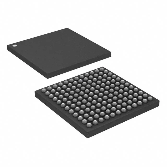
144-UFBGA package — footprint and routing notes
The 114 I/O count gives you room for a parallel LCD interface, external memory bus (EBI/EMI), and multiple serial peripherals simultaneously. Plan for a 4-layer or 6-layer stack-up with a dedicated ground plane under the BGA to maintain signal integrity on the high-speed QSPI and USB OTG lines.
That means it is still in volume production, supported by the manufacturer's full documentation, software ecosystem (STM32CubeMX, HAL/LL drivers), and distribution channel.