The 100 MHz Cortex-M4 includes a single-cycle multiply and a hardware FPU, so DSP-style filtering or FFTs run without a separate co-processor. For a control loop running at 10 kHz, you have roughly 10 000 cycles per iteration — enough for a PID with a biquad filter and some diagnostics. The Flash prefetch and instruction cache help keep the pipeline fed at this clock speed; just remember to set the Flash wait states correctly in the initialisation code (one wait state above 30 MHz, two above 60 MHz).
Memory sizing for the BOM decision
The Flash is enough for a FreeRTOS-based application with a TCP/IP stack and a modest file system; the RAM handles several large buffers (e.g., a 320x240 frame buffer for the LCD controller takes about 150 KB, leaving 100 KB for stack and heap). If your application needs more than 512 KB of code or a large data cache, you would step up to the STM32F412VE's 1 MB Flash sibling — but for most sensor-fusion and connectivity tasks, this memory split is well balanced.
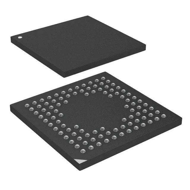
Package reality: 100-UFBGA
It is not a hand-solderable part — you need a stencil, reflow oven, and preferably X-ray inspection for the hidden joints.
This MCU includes a full set of peripherals: CANbus for industrial networks, USB OTG for host/device mode, multiple SPI and I²C for sensors and displays, an external memory interface (EBI/EMI) for parallel SRAM or NAND Flash, and a Quad-SPI for high-speed serial Flash. The 12-bit ADC with 16 channels covers analog inputs like potentiometers, current shunts, or thermistor bridges. The brown-out detect and POR circuits simplify the power supply design — no external supervisor needed for basic reset generation.
For new designs, this is a safe choice — no last-time-buy planning needed. If you need a dual-source hedge, the pin-compatible STM32F412VET6 in LQFP-100 is an official alternative, though the package footprint differs.