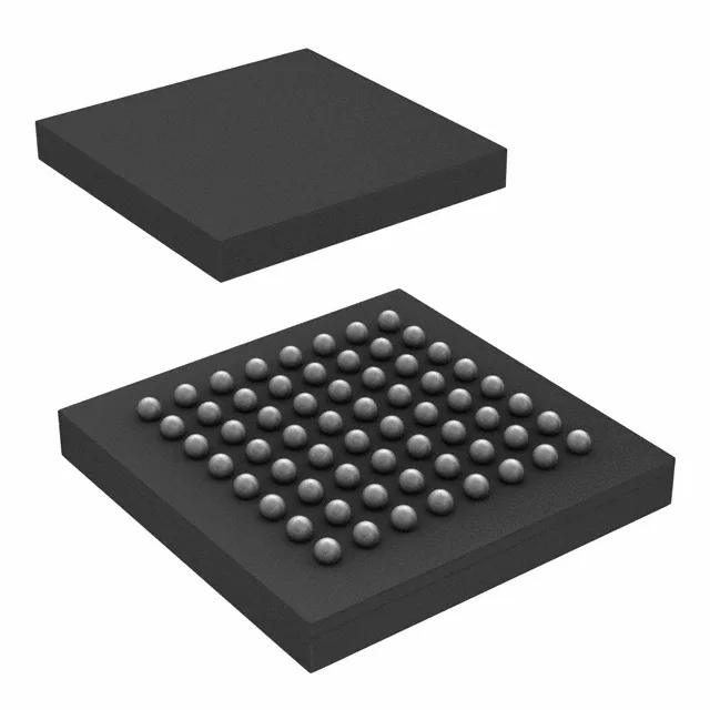
100 MHz Cortex-M4 with FPU in a 5x5 mm BGA
The STM32F410RBI6 is an STM32F4 series MCU built around an ARM Cortex-M4 core with single-precision FPU, clocked at 100 MHz. Part of ST's mainstream STM32F4 line, it targets industrial sensor nodes, motor-control interfaces, and IoT edge endpoints where the combination of DSP extensions and a compact BGA footprint matters more than the larger Flash densities in the sibling parts.
128 KB Flash — sizing the firmware budget
The 128 KB program memory (128K x 8) is the mid-range density option in the STM32F410 line. It fits a bootloader plus a moderate application stack — think sensor fusion with a FreeRTOS kernel, a TCP/IP stack stub, and a couple of peripheral drivers. If the project needs over-the-air update staging, the 32 KB SRAM leaves about 16 KB for runtime heap after the OS and comms buffers, so the OTA image size needs budgeting against the Flash sector erase granularity. The 128 KB density also keeps the per-unit cost below the 256 KB sibling, which matters for BOM-driven designs.
64-UFBGA (5x5 mm) — layout and assembly notes
That pitch requires at least a 4-layer PCB with microvia capability if you route all 50 I/O out without dog-boning. The small footprint is the main reason to pick this package over the LQFP-64 variant — it saves roughly 40% board area.
The internal oscillator and PLL are characterized across this range, but the 100 MHz speed grade assumes the flash wait state is set correctly — at 85°C and 3.0 V supply, the datasheet typically requires 1 wait state above 72 MHz. This is a firmware-configurable item during clock-tree initialization, not a hardware limit.
It lacks USB and CAN, so designs needing those will look at the STM32F412 or STM32F405 siblings. The 16-channel 12-bit ADC and single 12-bit DAC cover analog front-end needs for current sensing or audio output.
The STM32F4 series has been a long-running mainstream platform, so PCN risk is low for the near term. For dual-source resilience, the STM32F410CBx6 and STM32F410RBx6 share the same 64-UFBGA footprint and peripheral set, differing only in Flash density — a pin-compatible drop-in if the BOM can tolerate the spec change.