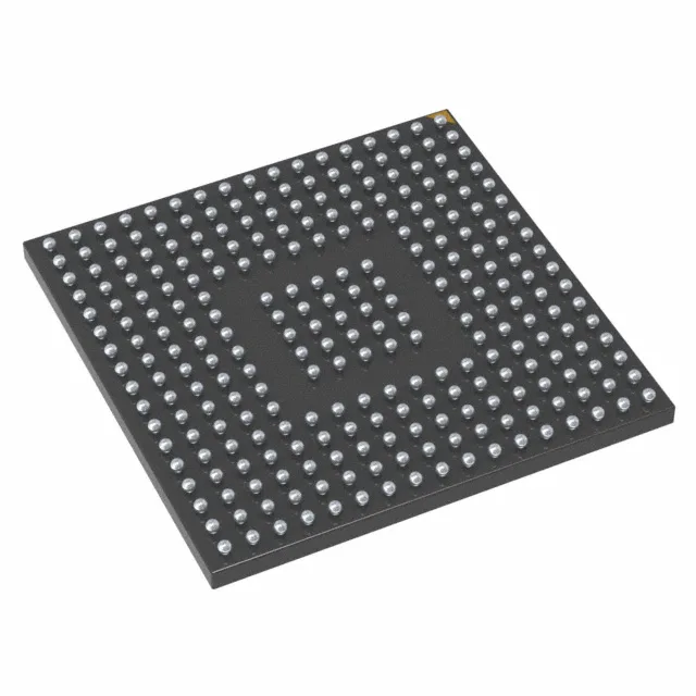
The 176+25 UFBGA (10x10 mm) package packs 140 I/O into a compact footprint, but the fine 0.5 mm ball pitch means the rework station needs an X-ray for post-reflow inspection.
512 KB Flash and 192 KB SRAM — sizing the application boundary
That's enough headroom for a TCP/IP stack with a small web server, a CANopen node with a few hundred objects, or a camera capture buffer for VGA frames. It won't hold a full GUI framebuffer plus a large data log — designs that need that should look at the STM32F429's larger SRAM or external SDRAM via the FMC. The 192 KB is organised as a single bank, so DMA transfers between peripherals and memory don't hit the same arbitration wall you'd see on dual-bank parts.
That means ST is still manufacturing this part in volume, so there's no last-time-buy clock ticking on the BOM. For a production run that spans two to three years, this MCU is a safe anchor — no forced redesign mid-cycle.