What this STM32F407IEH6 brings to a design
The STM32F407IEH6 is an STMicroelectronics STM32F4-series microcontroller built around an ARM Cortex-M4 core with FPU, clocked at 168 MHz. The peripheral set includes Ethernet MAC, two CAN 2.0B interfaces, USB OTG HS/FS, multiple SPI/I²C/UARTs, a 12-bit ADC with 24 channels, and a 12-bit DAC with two channels — a combination that suits industrial gateways, motor drives, and mid-range embedded systems that need both deterministic control and network connectivity.
The 168 MHz core speed, combined with the single-cycle multiply and hardware divide of the Cortex-M4, delivers enough compute headroom for single-precision DSP tasks like sensor fusion, FFT-based vibration analysis, or field-oriented control of a PMSM motor. The flash accelerator with adaptive real-time memory accelerator (ART Accelerator) means zero-wait execution from Flash at up to 168 MHz, so the headline clock is usable — not a theoretical number that stalls on instruction fetches.
Memory sizing for the firmware engineer
512 KB Flash is sufficient for a TCP/IP stack (LwIP or similar), a CANopen or EtherCAT slave library, and a moderate application layer — but if you are planning OTA firmware updates with a backup image, the usable Flash halves. The 192 KB SRAM divides into 128 KB on the main bus and 64 KB on the peripheral bus (CCM data RAM), which the core can access without bus contention. That CCM RAM is a good home for time-critical interrupt vectors or audio buffers.
Connectivity and peripheral fit
The USB OTG port can act as host for a USB flash drive or as device for firmware update over USB DFU. The DCMI (digital camera interface) is a less common feature at this price point, useful for vision-guided robotics or barcode scanning.
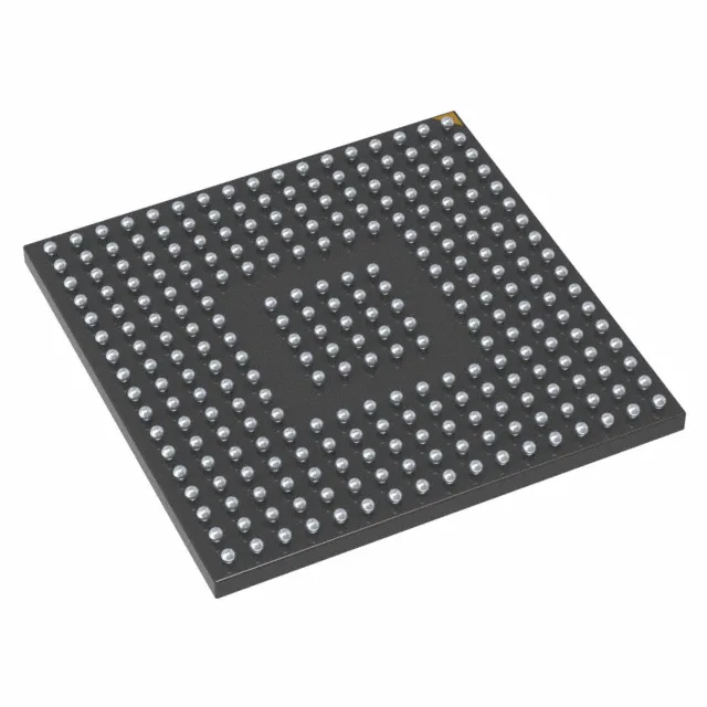
Housed in a 201-ball UFBGA (10x10 mm body, 0.5 mm pitch), the STM32F407IEH6 requires a 4-layer PCB with microvias or blind vias for fanout — the 0.5 mm pitch does not route cleanly on a 2-layer board. The 176+25 UFBGA variant (supplier device package) exposes 140 I/O, which is generous for a BGA this size.
The internal oscillator and POR/BOR circuitry reduce external component count in these environments.