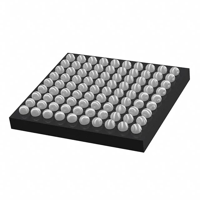
STM32F405OGY6WTR — 168 MHz Cortex-M4 in a wafer-level CSP
That package choice drives the board design: fine-pitch BGA-class assembly, no exposed pad for thermal relief, and the die is essentially the package — mechanical stress from PCB flex or reflow profile directly couples to the silicon. This is the variant to specify when board area is the binding constraint, not when through-hole or QFP rework convenience matters. On-chip data conversion includes 13 channels of 12-bit ADC and 2 channels of 12-bit DAC, which can eliminate a separate analog front-end IC in sensor-conditioning or closed-loop control applications.
This is not a full EOL — the manufacturer has not issued a last-time-buy cutoff — but it signals that the part is in a managed phase-out and will not be allocated for new project starts. For an existing BOM that already qualifies this WLCSP variant, NRND means the supply window is finite: remaining factory stock and independent-distributor inventory are the channels, and date-code freshness matters because the die-attach and underfill materials in a WLCSP have a shelf-life consideration beyond standard MSL handling. The broader STM32F405 family includes pin-compatible LQFP and BGA variants, but the WLCSP-specific ball map and mechanical footprint are unique to this OG package code. A BOM that relies on the 4.22 x 3.97 mm CSP footprint will need a board respin to migrate to any alternative package.
168 MHz and 1 MB Flash — what the ratings mean at the bench
The 168 MHz core clock is the maximum rated speed; reaching it requires setting the flash wait states to at least 3 cycles (per the STM32F4 reference manual) or the CPU hard-faults on the first instruction fetch outside the ART Accelerator cache. At this clock rate, the Cortex-M4 FPU and DSP extension execute single-cycle MAC operations, making the part viable for real-time FFT, motor-field-oriented control, or audio processing without a separate DSP. The 1 MB Flash is organized as 1M x 8 bits. Erase granularity is 128 KB sectors for the main block and 16 KB for the system memory — important when sizing an OTA update partition or a wear-leveled configuration store. The 192 KB SRAM is split across 128 KB of main SRAM and 64 KB of tightly-coupled CCM (core-coupled memory) accessible only by the CPU, not the DMA. CCM is the spot for time-critical interrupt vectors and stack data that cannot tolerate bus contention. At 168 MHz the active current draw is in the tens-of-milliamps range; the internal POR and BOR circuits handle brown-out sequencing without an external supervisor IC for most single-supply designs.
This is the standard STM32F4 temperature tier; the 125°C extended variant is a different order code. If your system sees sustained junction temperatures above 85°C, the WLCSP package's thermal resistance (no exposed pad) means you need to budget airflow or a heatsink interface to the PCB copper plane.