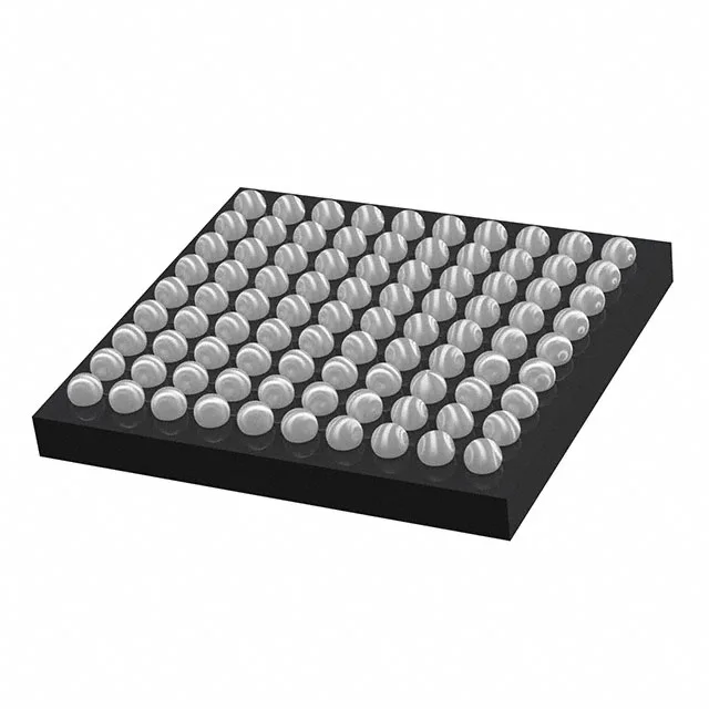
STMicroelectronics STM32F405OGY6VTR — Microcontrollers & Processors (MCU / MPU / DSP)

STM32F405OGY6VTR ARM Cortex-M4 MCU, 168 MHz, NRND

MPNSTM32F405OGY6VTR
NRND

STMicroelectronics STM32F405OGY6VTR, ARM Cortex-M4, 32-Bit Single-Core MCU, 168 MHz, 1 MB Flash, 192K x 8 RAM, 72 I/O, 90-WLCSP, -40°C ~ 85°C.

$7.8652Ref. price · indicative, final on quote
Independent supplier — new & surplus stockAuthenticity-screened · ESD-safe packingListing updated Jul 2026

Specifications

STM32F405OGY6VTR specifications
ParameterValue
SeriesSTM32F4
MountingSurface Mount
Oscillator typeInternal
Program memory typeFLASH
Voltage - supply (Vcc (Vdd))1.8V ~ 3.6V
Operating temperature-40°C ~ 85°C (TA)
Speed168MHz
PackageTape & Reel (TR)
RAM size192K x 8
Core size32-Bit Single-Core
PeripheralsBrown-out Detect/Reset, DMA, I²S, LCD, POR, PWM, WDT
ConnectivityCANbus, EBI/EMI, I²C, IrDA, LINbus, SPI, UART/USART, USB OTG
Number of i (O)72
Core processorARM® Cortex®-M4
Case90-UFBGA, WLCSP
Data convertersA/D 13x12b; D/A 2x12b
Program memory size1MB (1M x 8)

Product details

This is the official flag that ST has stopped actively promoting this exact WLCSP variant for new production builds. For an existing BOM line, this means the part remains available through the independent channel for ongoing production support, but any new board spin should target a current-recommended STM32F4 device. The NRND status does not trigger an immediate last-time-buy deadline, but it does put the clock on long-term availability — qualify an alternate before the next allocation cycle tightens supply.

168 MHz Cortex-M4 with 1 MB Flash — what it delivers

The 1 MB of on-chip Flash and 192 KB of SRAM give it the memory headroom for a real-time control stack with a modest communications protocol layer — think motor drive with field-oriented control, or a multi-protocol gateway handling CAN, USB OTG, and Ethernet simultaneously. The 72 I/O lines, mapped through the 90-ball WLCSP, provide enough GPIO for parallel display interfaces or a sensor array without external port expanders.

90-WLCSP — footprint and rework considerations

This gives the smallest footprint for the 72-I/O count, but it demands a controlled SMT process: the solder balls are directly on the die pads, so the board-side pad design, solder paste volume, and reflow profile must match ST's WLCSP application note. The package is not rework-friendly — a misaligned placement typically scrapes the board. For a production line already running WLCSP, this is a known process; for a first-time user, budget for a prototype build to validate the stencil and profile.

Frequently asked questions

Is STM32F405OGY6VTR obsolete?

It is not yet discontinued, but ST has signaled that this specific WLCSP variant is no longer the recommended choice for new designs. Existing production can continue with sourced inventory through the independent channel.

What is the replacement for STM32F405OGY6VTR?

The NRND designation means ST expects designers to move to a current STM32F4 device in a similar package and memory tier — typically the STM32F405 or STM32F407 family in a more widely supported package like LQFP or BGA. For a pin-compatible drop-in, verify the package footprint and ball map against the current STM32F4 WLCSP options in ST's product selector.